
Time domain interleaved ADC multi-phase clock generation circuit
A multi-phase clock and generation circuit technology, applied in electrical components, analog-to-digital converters, code conversion, etc., can solve the problems of poor flexibility of clock duty cycle high-level overlap control, timing continuity problems, complexity, etc. Achieve the effects of good timing relationship, adjustable high-level overlap, and adjustable duty cycle
- Summary
- Abstract
- Description
- Claims
- Application Information
AI Technical Summary
Problems solved by technology
Method used
Image

Examples
Embodiment 1
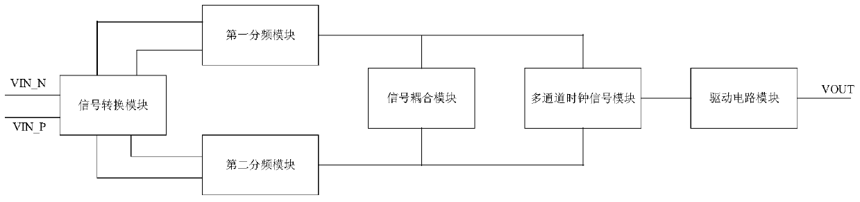
[0062] See figure 1 , figure 1 It is a schematic structural diagram of a time-domain interleaved ADC multi-phase clock generation circuit provided by an embodiment of the present invention. This embodiment provides a time-domain interleaved ADC multi-phase clock generation circuit, the time-domain interleaved ADC multi-phase clock generation circuit includes a signal conversion module, a first frequency division module, a second frequency division module, a signal coupling module, a multi-channel Clock signal module, drive circuit module, wherein,
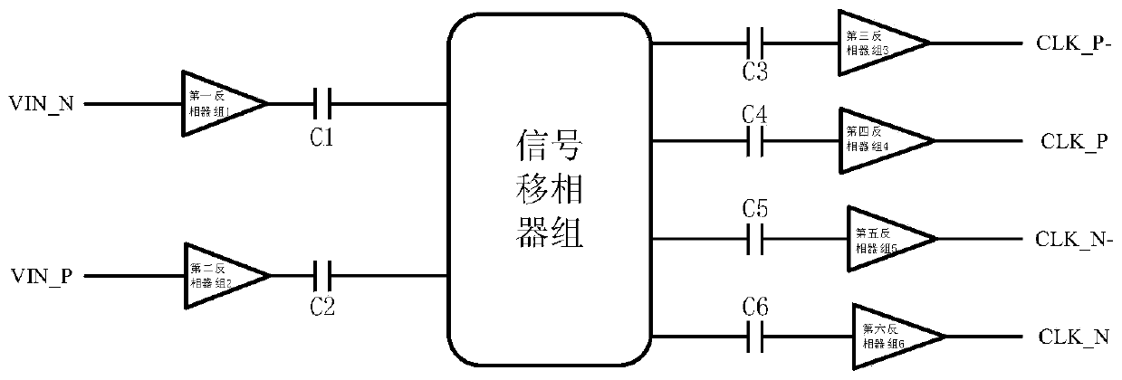
[0063] A signal conversion module, configured to generate a first output signal, a second output signal, a third output signal and a fourth output signal according to the first input signal and the second input signal;
[0064] The first frequency division module is connected to the signal conversion module, and is used for performing frequency division processing on the first output signal and the second output signal to obtain ...
PUM
 Abstract
Description
Claims
Application Information