
Light emitting diode apparatus and method of manufacturing the same

A technology of light-emitting diodes and electrodes, which is applied in the direction of electrical components, circuits, semiconductor devices, etc., can solve the problems of luminous efficiency reduction, heat generation, etc., and achieve the effects of improving luminous efficiency and current crowding effect

Active Publication Date: 2020-04-21
SAMSUNG ELECTRONICS CO LTD
View PDF15 Cites 0 Cited by
  • Summary
  • Abstract
  • Description
  • Claims
  • Application Information

AI Technical Summary

Problems solved by technology

[0003] However, in the light-emitting diode of the related art, the n-type electrode and the p-type electrode that supply electrons and holes are respectively biased to one region in the light-emitting diode, and therefore, the luminous efficiency increases with the difference between the n-type electrode and the p-type electrode. Decreases exponentially with increasing distance
In addition, local heating occurs near where the electrodes are located

Method used


Image

  • Light emitting diode apparatus and method of manufacturing the same
  • Light emitting diode apparatus and method of manufacturing the same
  • Light emitting diode apparatus and method of manufacturing the same

Examples


Embodiment Construction

[0036] Specific example embodiments are illustrated in the drawings and described in the detailed description. However, it should be understood that the present disclosure is not limited to specific example embodiments, but includes all modifications, equivalents, and substitutions that do not depart from the scope and spirit of the present disclosure. Regarding the description of the drawings, the same or similar reference numerals may be used for similar constituent components.

[0037] It should be understood that when a component (eg, a first component) is "coupled / coupled (operatively or communicatively)" or "connected" to another component (eg, a second component), the component A component may be directly coupled to / coupled to another component, and an intermediate component (eg, a third component) may exist between the component and another component. Instead, it should be understood that when a component (eg, a first component) is "directly coupled to / coupled to" or ...


PUM


Abstract

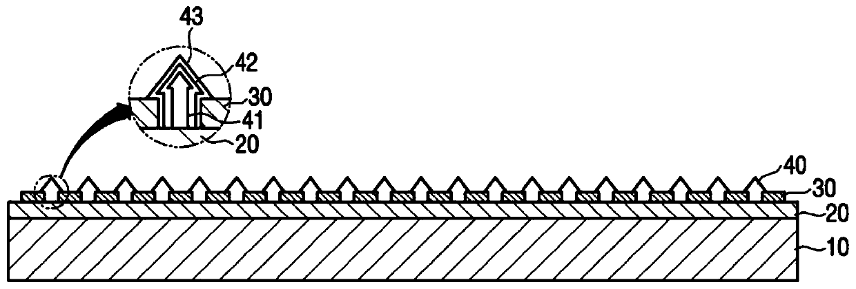
A method of manufacturing a light emitting diode is provided. The method includes forming a semiconductor layer on a substrate, forming a mask layer including a plurality of grooves on the semiconductor layer, forming a plurality of nanostructures in the plurality of grooves, respectively, forming an etched region by etching an outer region of the semiconductor layer and an inner region of the semiconductor layer different from the outer region, forming a first electrode on the etched region of the semiconductor layer, forming an insulation layer on the first electrode, and forming a second electrode on the insulation layer and the plurality of nanostructures.

Description

technical field [0001] Apparatuses and methods consistent with the present disclosure relate to light emitting diodes and methods of fabricating light emitting diodes, and in particular to light emitting diodes comprising nanostructures and methods of fabricating light emitting diodes comprising nanostructures. Background technique [0002] Light emitting diodes (LEDs) have the advantages of long life, low power consumption, and fast response, and thus are used in various display devices and lighting devices. In recent years, light emitting diodes including nanostructures have been used to increase the light emitting area. [0003] However, in the light-emitting diode of the related art, the n-type electrode and the p-type electrode that supply electrons and holes are respectively biased to one region in the light-emitting diode, and therefore, the luminous efficiency increases with the difference between the n-type electrode and the p-type electrode. Decreases exponentiall...

Claims


Application Information

Patent Timeline
Patent Type & Authority Applications(China)
IPC IPC(8): H01L33/00H01L33/36H01L33/10H01L33/62
CPCH01L33/18H01L33/24H01L33/385H01L33/405H01L33/44H01L33/007H01L33/08H01L33/20H01L33/382H01L33/46H01L33/62H01L33/005H01L33/36H01L33/0008H01L33/10H01L33/60
Inventor 金载石姜镇熙姜智薰
Owner SAMSUNG ELECTRONICS CO LTD
Learn More