Driving device of light emitting diode array panel and driving method thereof

A technology of light-emitting diodes and array panels, which is applied to instruments, static indicators, etc., can solve the problems of easy drift, uneven brightness of display devices, and affect the display effect, so as to solve inaccurate compensation, improve uniformity and accuracy , the effect of improving uniformity

Active Publication Date: 2020-04-24
SHENZHEN CHINA STAR OPTOELECTRONICS SEMICON DISPLAY TECH CO LTD
View PDF19 Cites 1 Cited by
  • Summary
  • Abstract
  • Description
  • Claims
  • Application Information

AI Technical Summary

Problems solved by technology

Usually, the driving current Ids of the LED is large, so the driving thin film transistor T1 usually needs to use Indium Gallium Zinc Oxide (IGZO) semiconductor material, and for the transistor, the length and width of the channel can reflect The probability of carriers being trapped during the migration process, when the aspect ratio is larger, the threshold voltage Vth of the TFT is very easy to drift. Since the driving thin film transistor T1 is in the saturation region, the driving current Ids is very susceptible to threshold voltage Vth drift The influence of different areas of the display device causes uneven luminance, which affects the display effect

Method used


Image

  • Driving device of light emitting diode array panel and driving method thereof
  • Driving device of light emitting diode array panel and driving method thereof
  • Driving device of light emitting diode array panel and driving method thereof

Examples


Embodiment Construction

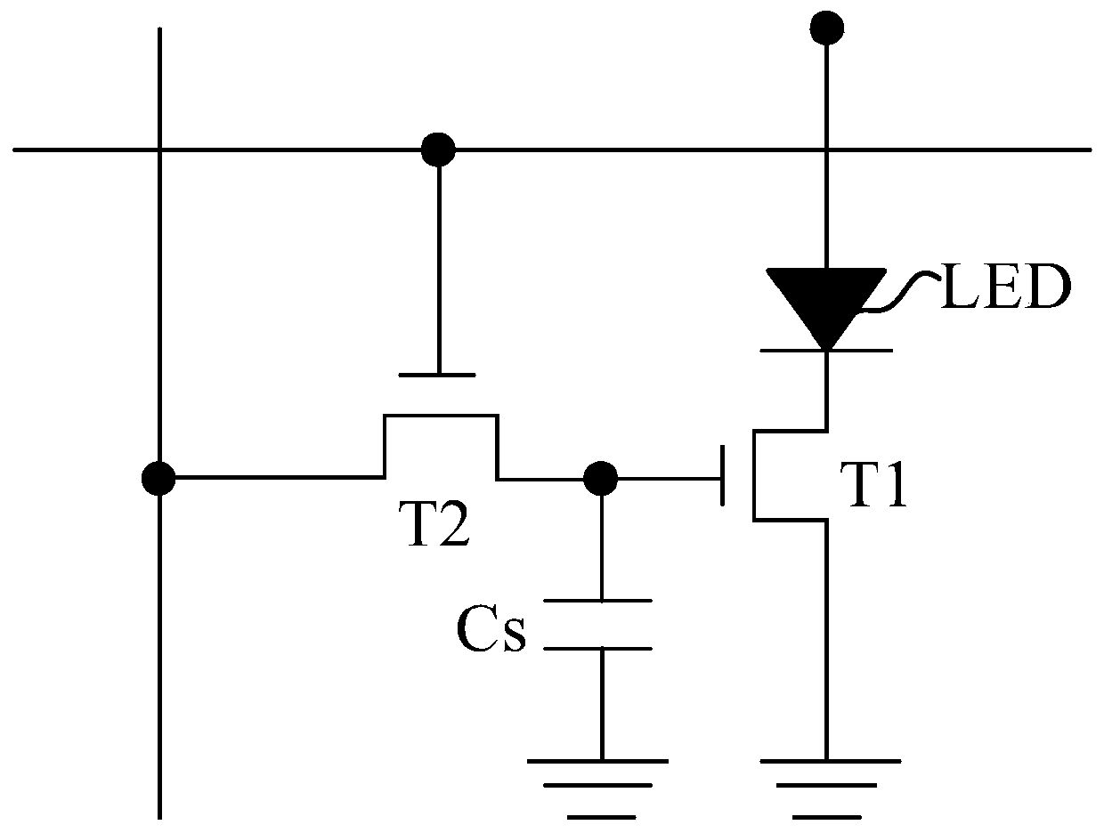
[0048] In order to make the purpose, technical solution and advantages of the present invention clearer, the present invention will be further described in detail below in conjunction with the accompanying drawings, please refer to the drawings in the accompanying drawings, wherein the same component symbols represent the same components, the following description is Based on the particular embodiment of the invention shown, it should not be construed as limiting the invention to other embodiments not detailed herein. The word "embodiment" as used in this specification means an example, instance or illustration. Furthermore, as used in this specification and the appended claims, the article "a" or "an" may generally be construed as "one or more" unless specified otherwise or clear from the context in the singular.

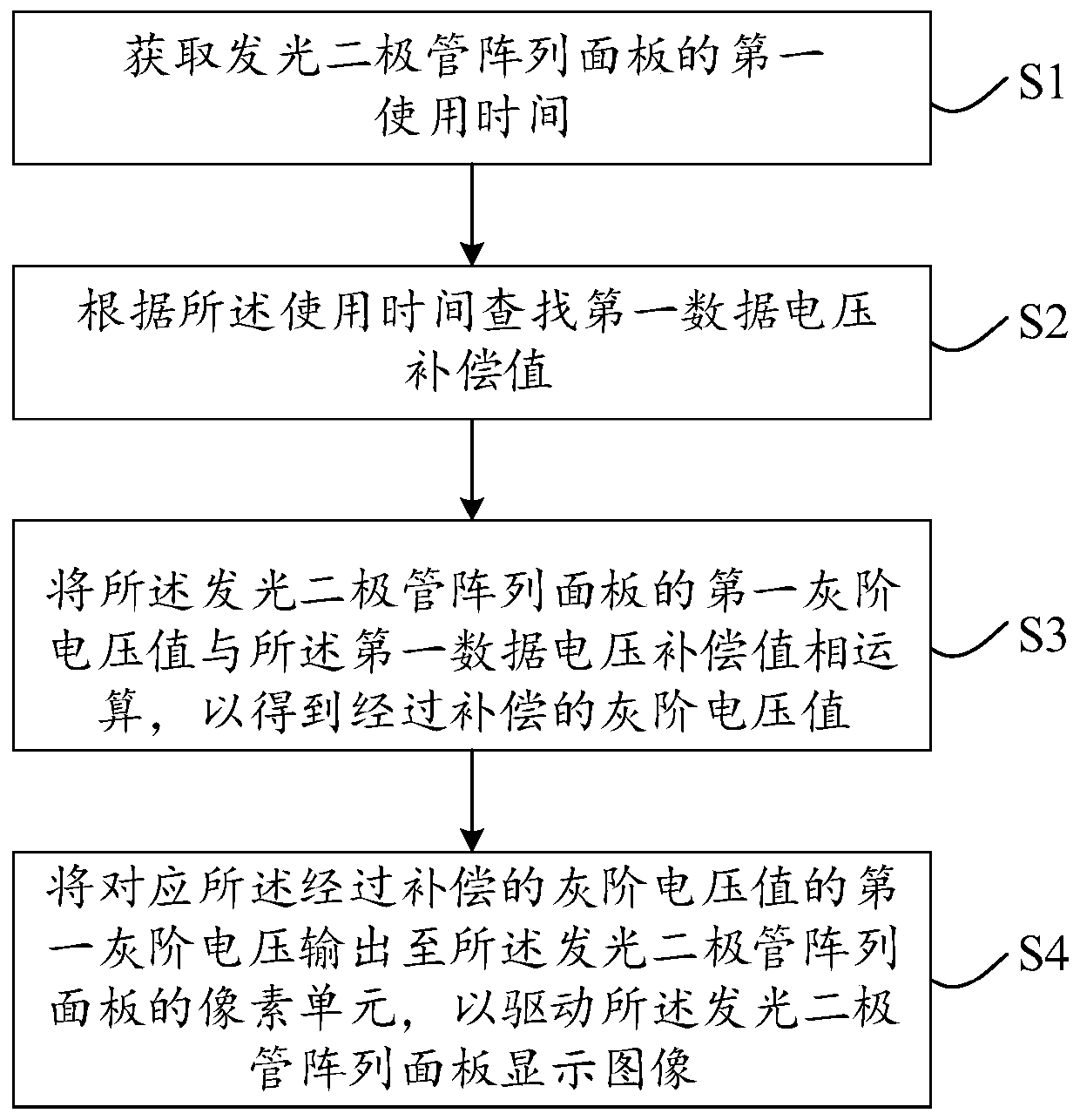
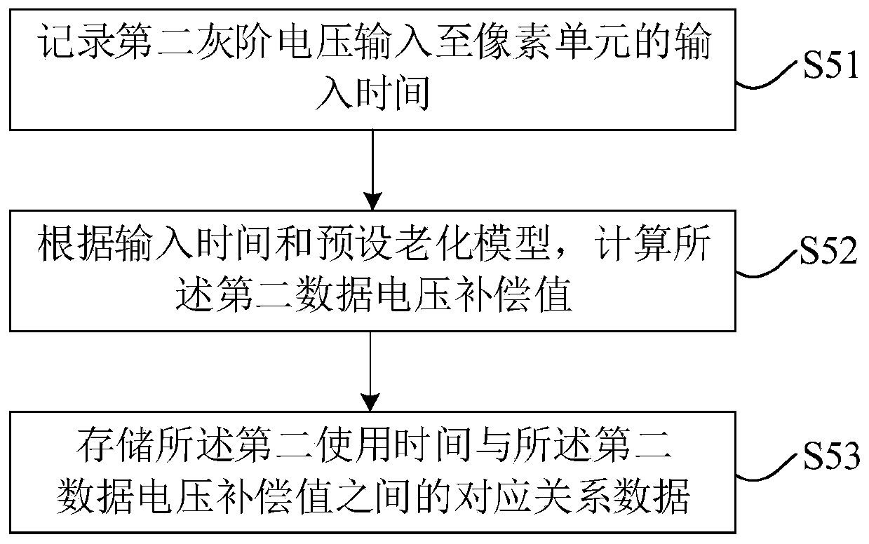
[0049] Such as figure 2 As shown, an embodiment of the present invention provides a driving method of a light emitting diode array panel, the driving method comp...


PUM


Abstract

The invention discloses a driving device and a driving method of a light emitting diode array panel. The driving method comprises the following steps: acquiring first use time of the light emitting diode array panel; searching a first data voltage compensation value according to the first use time; calculating a first gray-scale voltage value of the light emitting diode array panel and the first data voltage compensation value to obtain a compensated gray-scale voltage value; and outputting the first gray-scale voltage corresponding to the compensated gray-scale voltage value to a pixel unit of the light emitting diode array panel so as to drive the light emitting diode array panel to display an image. The problem that the driving current Ids is drifted by the threshold voltage Vth to cause non-uniform luminance of different regions of the display device can be solved, so that the uniformity of the luminance of different regions is improved.

Description

technical field [0001] The invention relates to the field of display technology, in particular to a driving device and a driving method for a light emitting diode array panel. Background technique [0002] A light emitting diode (LED, Light Emitting Diode) display device is composed of a pixel array, and each pixel includes a light emitting diode and a pixel driving circuit for driving the light emitting diode. Such as figure 1 As shown, a common pixel driving circuit is composed of a data writing thin-film transistor (TFT, Thin-Film Transistor) T2, a driving thin-film transistor T1, and a capacitor Cs. Usually, the driving current Ids of the LED is large, so the driving thin film transistor T1 usually needs to use Indium Gallium Zinc Oxide (IGZO) semiconductor material, and for the transistor, the length and width of the channel can reflect The probability of carriers being trapped during the migration process, when the aspect ratio is larger, the threshold voltage Vth of...

Claims


Application Information

Patent Timeline
Patent Type & Authority Applications(China)
IPC IPC(8): G09G3/32
CPCG09G3/32
Inventor 蔡振飞
Owner SHENZHEN CHINA STAR OPTOELECTRONICS SEMICON DISPLAY TECH CO LTD
Why Eureka
Try Eureka