Supercharge Your Innovation With Domain-Expert AI Agents!

Semiconductor test structure and test method

A test structure and semiconductor technology, which is applied in semiconductor/solid-state device testing/measurement, semiconductor devices, semiconductor/solid-state device components, etc., can solve problems such as inaccurate positioning of short-circuit failure points, and save human resources and machine resources , accurate positioning, and the effect of improving test efficiency

Active Publication Date: 2021-09-03
SHANGHAI HUALI MICROELECTRONICS CORP
View PDF5 Cites 0 Cited by
  • Summary
  • Abstract
  • Description
  • Claims
  • Application Information

AI Technical Summary

Problems solved by technology

[0005] The object of the present invention is to provide a semiconductor test structure and test method to solve the problem of inaccurate positioning when locating the short-circuit failure point of a repeated, large-area test structure

Method used


Image

  • Semiconductor test structure and test method
  • Semiconductor test structure and test method
  • Semiconductor test structure and test method

Examples


Embodiment Construction

[0034] The semiconductor testing structure and testing method proposed by the present invention will be further described in detail below with reference to the accompanying drawings and specific embodiments. The advantages and features of the present invention will become more apparent from the following description. It should be noted that, the accompanying drawings are all in a very simplified form and in inaccurate scales, and are only used to facilitate and clearly assist the purpose of explaining the embodiments of the present invention. Furthermore, the structures shown in the drawings are often part of the actual structure. In particular, each drawing needs to show different emphases, and sometimes different scales are used.

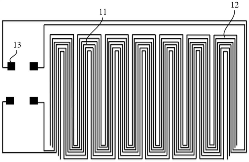
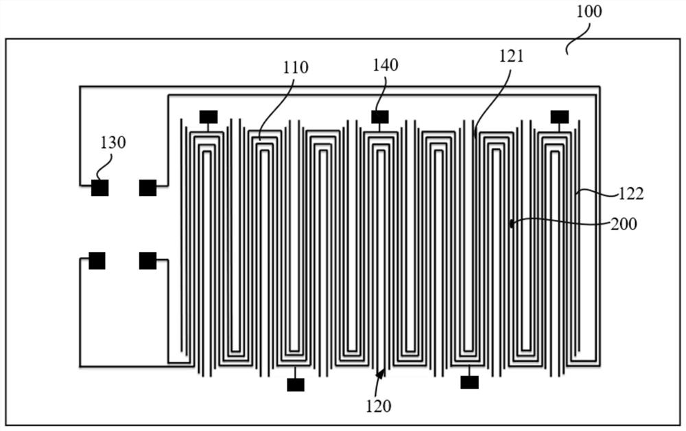
[0035] The present invention provides a semiconductor test structure, refer to figure 2 , image 3 and Figure 4 , figure 2 is a schematic diagram of a semiconductor test structure according to an embodiment of the present invention, imag...


PUM

PropertyMeasurementUnit
areaaaaaaaaaaa

Abstract

The present invention provides a semiconductor test structure, comprising: a main test structure, an auxiliary test structure, two groups of first test pads, at least two second test pads, a first dielectric layer, and the second test pads It is electrically connected with the main test structure so that the main test structure is electrically tested through two of the second test pad segments; further, the present invention also provides a short-circuit test method, including: using a resistor Coarse positioning of the defect point by the ratio method to determine the serpentine structure where the defect point is located; fine positioning of the defect point through the second test pad and using the electric resistance change technology; observing the defect point And collect its SEM image; prepare TEM sample to determine the cause of the short circuit in the main test structure. By adding the second test pad, the main test structure can be divided into multiple test structures, so that each test structure can be independently tested for electrical performance, so that defects can be found effectively.

Description

technical field [0001] The invention relates to the field of semiconductor testing, in particular to a semiconductor testing structure and a testing method. Background technique [0002] The semiconductor manufacturing process is divided into a front-end device process and a back-end metal interconnect process. The function of the back-end metal interconnect layer in the back-end metal interconnect process is to lead out the front-end device in the front-end device process for testing or work. In the semiconductor manufacturing process, short-circuit failure or open-circuit failure often occurs in the back-end metal interconnect lines, which are mainly due to design problems and process problems. In order to evaluate the design structure and monitor the stability of the online process, the complex product structure is extracted separately or reorganized into a repeating, large-area, and easy-to-test structure by using the structure as a unit. A large number of corresponding...

Claims


Application Information

Patent Timeline
Patent Type & Authority Patents(China)
IPC IPC(8): H01L23/58H01L21/66
CPCH01L22/14H01L23/58
Inventor 武城杨领叶段淑卿高金德
Owner SHANGHAI HUALI MICROELECTRONICS CORP
Features
  • R&D
  • Intellectual Property
  • Life Sciences
  • Materials
  • Tech Scout
  • Unparalleled Data Quality
  • Higher Quality Content
  • 60% Fewer Hallucinations
Learn More