Eureka AIR delivers breakthrough ideas for toughest innovation challenges, trusted by R&D personnel around the world.

Method for optimizing combination of conductive atomic force microscope and digital source meter

An atomic force microscope and digital source meter technology, applied in scanning probe microscopy, instruments, measuring devices, etc., can solve the cumbersome process of instrument connection, the inability to observe the local topography of the sample, and the inability to further analyze the physical properties of the sample. Information and other issues to achieve the effect of reducing time costs

Pending Publication Date: 2020-05-08
SUZHOU UNIV
View PDF5 Cites 0 Cited by
  • Summary
  • Abstract
  • Description
  • Claims
  • Application Information

AI Technical Summary

Problems solved by technology

However, in the actual operation process, the process of connecting the instrument is cumbersome and it is impossible to observe the local topography of the sample after the electrical performance is characterized by a digital source meter, which makes it impossible to further analyze the relevant physical information of the sample.

Method used


Image

  • Method for optimizing combination of conductive atomic force microscope and digital source meter
  • Method for optimizing combination of conductive atomic force microscope and digital source meter
  • Method for optimizing combination of conductive atomic force microscope and digital source meter

Examples


Embodiment Construction

[0017] The specific operation process of the present invention will be described in detail below. As a part of this description, the principle of the present invention will be described in detail through specific case explanations. Other aspects, features and other advantages of the present invention will be realized through the detailed explanation of this specific case. become clearer. However, the embodiments of the present invention are not limited to the specific embodiments listed below.

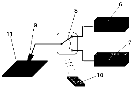
[0018] Such as figure 1 As shown, a method for optimizing the combination of a conductive atomic force microscope and a digital source meter is to connect the conductive module 6 of the conductive atomic force microscope to the digital source meter 7 through a single-pole double-throw radio frequency switch 8, so that the probe placed on the sample 11 during detection One of the pins 9 is connected to the conductive module 6 or the digital source meter 7 of the conductive atomic force...


PUM


Abstract

The invention relates to a method for optimizing combination of a conduction atomic force microscope (CAFM) and a digital source meter. A conductive module (CAFM Mode) and a digital source meter of aconductive atomic force microscope are connected with a conductive atomic force microscope through a single-pole double-throw radio frequency switch, so that a probe is selectively connected with theconductive module of the conductive atomic force microscope or the digital source meter. According to the method for combining a conductive atomic force microscope and a digital source meter, a novelsystem accessory is created and applied to the conductive atomic force microscope. The conductive atomic force microscope can be freely switched to different modes (CAFM mode or source meter), the position of the needle tip is not changed in the switching process, and the same area of the test sample can be represented at the same time, so that the original defects of the AFM instrument in use aregreatly overcome, technicians in the field are simpler, more convenient and more efficient in the experimental operation process, and the time cost of the scientific research personnel can be effectively reduced.

Description

technical field [0001] The invention relates to a measurement technique for local electrical properties and morphology features, in particular to a method for optimizing the combined use of a conductive atomic force microscope and a digital source meter. Background technique [0002] The invention of the scanning tunneling microscope enables humans to observe the arrangement of individual atoms on the surface of a material for the first time. It has a wide range of applications in various fields such as material science and life science. But it has its own limitations - it cannot analyze insulating materials. The advent of the atomic force microscope in 1986 brought the analysis of nanotechnology and materials in the scientific research field to a new level. [0003] In recent years, with the development of nanomaterials, organometallic composites, and nanoelectronic devices, conductive atomic force microscope (CAFM) has become a hot research tool for studying the local cond...

Claims


Application Information

Patent Timeline
Patent Type & Authority Applications(China)
IPC IPC(8): G01Q60/24G01Q30/00
CPCG01Q60/24G01Q30/00
Inventor 马尔科·维勒纳郭碧雨马里奥·兰扎
Owner SUZHOU UNIV
Why Eureka
Eureka Blog
Learn More