
A heteroplane structure Gaas photoconductive switch based on graphene interface layer and its preparation process
A photoconductive switch, graphene layer technology, applied in sustainable manufacturing/processing, semiconductor device, final product manufacturing and other directions, can solve the problems of short life, easy burnout, uneven heat dissipation of switching devices, and achieve good heat dissipation performance, The effect of high life and clear process
- Summary
- Abstract
- Description
- Claims
- Application Information
AI Technical Summary
Problems solved by technology
Method used
Image

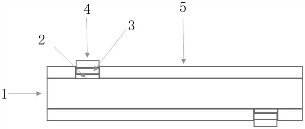
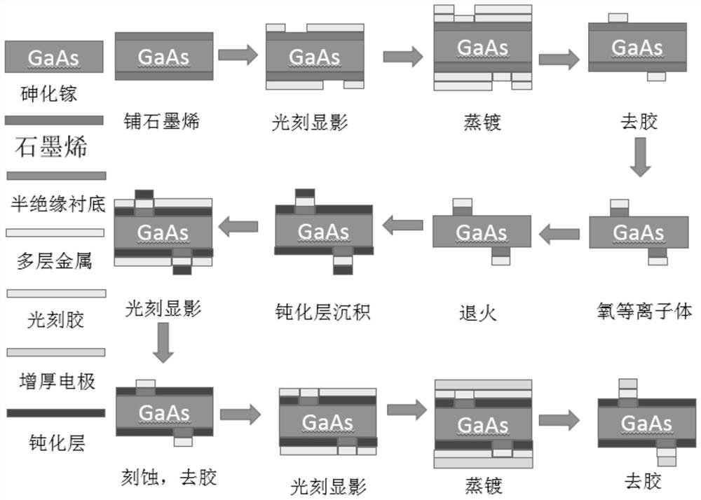
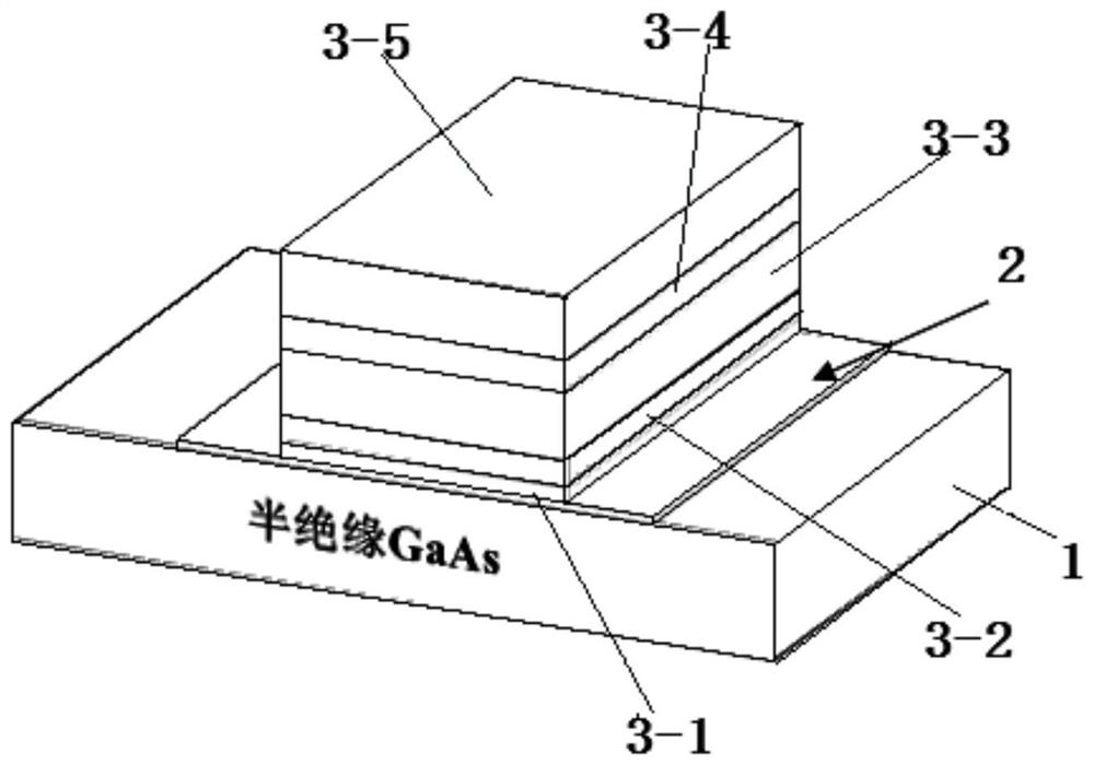
Examples
Embodiment 1
[0087] Select a semi-insulating gallium arsenide double-polished wafer with a crystal orientation , with a thickness of 600 μm, and use acetone, sulfuric acid and other processes to clean the surface of the gallium arsenide to remove surface impurities.
[0088] 1) Preparation of composite structure of CVD graphene and gallium arsenide
[0089] On a Cu foil with a thickness of 25 μm, graphene is grown by CVD, and the graphene is transferred to a semi-insulating GaAs surface by a pulling method to obtain a first composite structure.
[0090] 2) Graphicalize the first composite structure:
[0091] The first photolithography (front and back):
[0092] (1) Apply photoresist AZ-5214 (2) Uniform glue (3) Pre-baking (4) Exposure (5) Development (6) Post-baking (7) UVO to remove residual glue;
[0093] 3) Then make five layers of metal (front and back) on the surface as electrodes (Ni layer, Ge layer, Au layer, Ni layer and Au layer). The total thickness of the five layers of metal ...
Embodiment 2
[0104] Select a four-inch gallium arsenide double-polished wafer with crystal orientation , resistivity ≥ 10Ωcm, thickness 600μm, use acetone, sulfuric acid and other processes to clean the surface of gallium arsenide to remove surface impurities.
[0105] 1) Preparation of composite structure of CVD graphene and gallium arsenide
[0106] On a Cu foil with a thickness of 25 μm, graphene is grown by CVD, and the graphene is transferred to a semi-insulating GaAs surface by a pulling method to obtain a first composite structure.
[0107] 2) Graphicalize the first composite structure:
[0108] The first photolithography (front and back):
[0109] (1) Apply photoresist AZ-5214 (2) Uniform glue (3) Pre-baking (4) Exposure (5) Development (6) Post-baking (7) UVO to remove residual glue;
[0110] 3) Then make five layers of metal (front and back) on the surface as electrodes (Ni layer, Ge layer, Au layer, Ni layer and Au layer). The total thickness of the five layers of metal is 296...
Embodiment 3
[0121] Select a four-inch gallium arsenide double-polished wafer with crystal orientation , resistivity ≥ 10Ωcm, thickness 600μm, use acetone, sulfuric acid and other processes to clean the surface of gallium arsenide to remove surface impurities.
[0122] 1) Preparation of composite structure of CVD graphene and gallium arsenide
[0123] On a Cu foil with a thickness of 25 μm, graphene is grown by CVD, and the graphene is transferred to a semi-insulating GaAs surface by a pulling method to obtain a first composite structure.
[0124] 2) Graphicalize the first composite structure:
[0125] The first photolithography (front and back):
[0126] (1) Apply photoresist AZ-5214 (2) Uniform glue (3) Pre-baking (4) Exposure (5) Development (6) Post-baking (7) UVO to remove residual glue;
[0127] 3) Then make five layers of metal (front and back) on the surface as electrodes (Ni layer, Ge layer, Au layer, Ni layer and Au layer). The total thickness of the five layers of metal is 296...
PUM
| Property | Measurement | Unit |
|---|---|---|
| thickness | aaaaa | aaaaa |
| thickness | aaaaa | aaaaa |
| thickness | aaaaa | aaaaa |
Abstract
Description
Claims
Application Information