Inductor and manufacturing method thereof

A production method and technology of inductance, which is applied in the direction of inductors, circuits, electrical components, etc., can solve the problem that it is difficult to achieve high inductance value and high quality factor at the same time in planar inductance, and achieve the effect of good quality factor and large inductance value

Inactive Publication Date: 2020-05-12
福建省福联集成电路有限公司
View PDF6 Cites 0 Cited by
  • Summary
  • Abstract
  • Description
  • Claims
  • Application Information

AI Technical Summary

Problems solved by technology

[0003] Therefore, it is necessary to provide an inductor and its manufacturing method to solve the problem that the existing planar inductors are difficult to achieve high inductance and high quality factor at the same time

Method used


Image

  • Inductor and manufacturing method thereof
  • Inductor and manufacturing method thereof
  • Inductor and manufacturing method thereof

Examples


Embodiment Construction

[0036] In order to explain in detail the technical content, structural features, achieved goals and effects of the technical solution, the following will be described in detail in conjunction with specific embodiments and accompanying drawings.

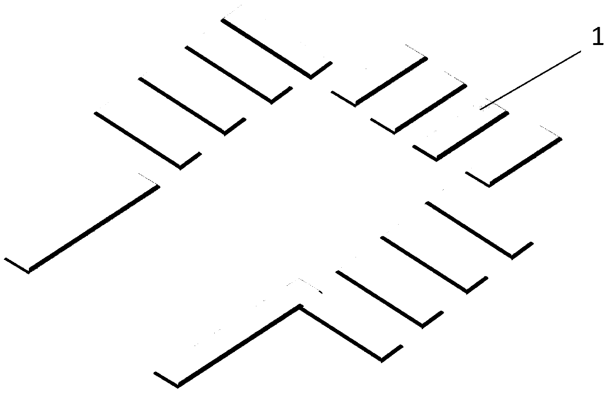
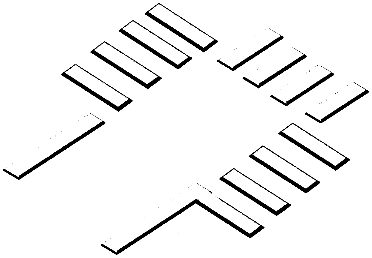
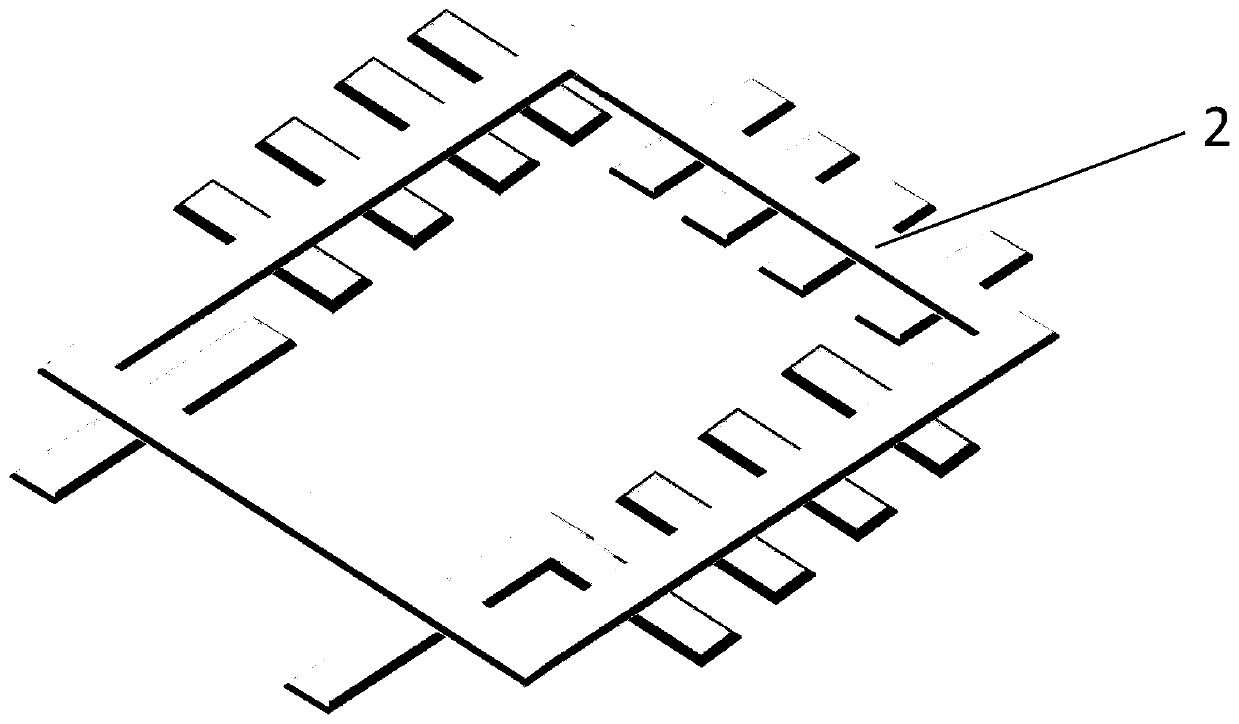
[0037] see Figure 1 to Figure 6 , this embodiment provides a method for manufacturing an inductor, which can generally be manufactured on an epitaxial wafer of a semiconductor device. The method comprises the following steps: depositing the first metal layer 1 of the inductor, the first metal layer of the inductor includes a plurality of discrete metal segments, and the formed structure is as follows figure 1 shown. Then deposit the first nitride layer on the first metal layer of the inductor, so that the first nitride covers each metal segment, such as figure 2 shown. The nitride of the present invention plays the role of insulation, such as silicon nitride and the like. Then deposit the inductor second metal layer 2 on the fir...


PUM


Abstract

The invention discloses an inductor and a manufacturing method thereof. The method comprises the following steps: depositing an inductance first metal layer, wherein the inductance first metal layer comprises a plurality of discrete metal sections; depositing a first nitride layer on the inductance first metal layer; depositing an inductance second metal layer on the first nitride layer, wherein the inductance second metal layer stretches across the middle position of the metal section; depositing a second nitride layer on the inductance second metal layer; forming openings on first nitrides at the two ends of the metal section; and manufacturing an air bridge by taking the openings as piers, so that different metal sections are connected end to end, wherein the second inductance metal layer is wound by an inductance coil formed by the metal sections and the air bridge. According to the technical scheme, the three-dimensional inductor can be manufactured, the quality factor is good under the high-frequency condition, and the inductor has large inductance.

Description

technical field [0001] The invention relates to the field of manufacturing inductors on semiconductor devices, in particular to an inductor and a manufacturing method thereof. Background technique [0002] In the prior art, most of the planar integrated inductors are used. With the complexity of the circuit application, the traditional integrated inductors cannot show good characteristics; the filter circuit integrated with the traditional inductors cannot filter out the disturbance generated by the electromagnetic field between the transmission lines. mode currents, causing disturbances on the load. In addition, in the prior art, it is difficult to simultaneously achieve a high inductance value and a high quality factor Q value due to the limitations of the manufacturing process and materials of the integrated circuit for the integrated inductor. The manufacturing process of the inductor in the prior art is as follows: first, the substrate is firstly subjected to vapor dep...

Claims


Application Information

Patent Timeline
Patent Type & Authority Applications(China)
IPC IPC(8): H01L23/64
CPCH01L28/10
Inventor 林豪王潮斌詹智梅陈智广陈东仰林张鸿林伟铭
Owner 福建省福联集成电路有限公司
Why Eureka
Try Eureka