Defect detection device applied to curved screen

A defect detection and curved screen technology, which is applied in measuring devices, optical testing of flaws/defects, and material analysis through optical means, can solve problems such as not being on the same level, poor screen imaging consistency, and defect detection efficiency. Reduced time, good imaging consistency, and improved operational efficiency

Pending Publication Date: 2020-05-15
WUHAN JINGLI ELECTRONICS TECH +1
View PDF0 Cites 12 Cited by
  • Summary
  • Abstract
  • Description
  • Claims
  • Application Information

AI Technical Summary

Problems solved by technology

like figure 1 As shown, the most common way to detect the curved surface is to use the current single front-facing camera to shoot. For the curved surface, a mirror is added to reflect the curved surface to the upper surface, so that the official camera can capture both the curved surface and the surface at one time. The screen part, but there is a problem: because the surface part 2 is not on the same level as the part of the screen plane 1
Therefore, in on-site applications, it is necessary to focus twice, one for the focus plane area and one for the curved surface. This method will result in twice the imaging time on site and reduce the efficiency of defect detection.
Especially in batch imaging, it is necessary to control the lens to switch the focus position back and forth when each sample is tested. Due to the focus accuracy problem, the focus position is switched back and forth, and the imaging consistency of different screens is poor.

Method used


Image

  • Defect detection device applied to curved screen
  • Defect detection device applied to curved screen
  • Defect detection device applied to curved screen

Examples


Embodiment Construction

[0022] In order to make the object, technical solution and advantages of the present invention clearer, the present invention will be further described in detail below in conjunction with the accompanying drawings and embodiments. It should be understood that the specific embodiments described here are only used to explain the present invention, not to limit the present invention. In addition, the technical features involved in the various embodiments of the present invention described below can be combined with each other as long as they do not constitute a conflict with each other.

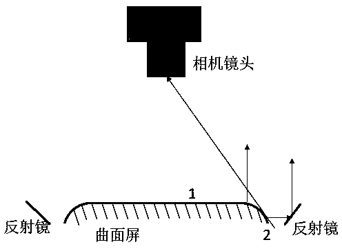
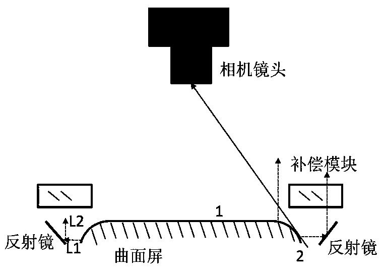
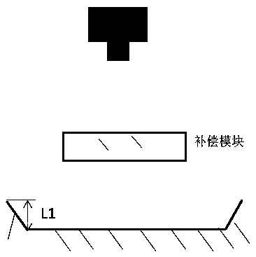
[0023] An embodiment of the present invention provides a defect detection device applied to a curved screen, which can perform imaging on the curved screen once. Curved screens include flat and curved surfaces, and can be convex screens, concave screens, or other screens that combine convex and concave surfaces.

[0024] The defect detection device includes: a camera, a detection module and an ...


PUM


Abstract

The invention discloses a defect detection device applied to a curved screen, and the curved screen comprises a plane and a curved surface, and the defect detection device is characterized by comprising a camera, a detection module and an optical path extension compensation module; the camera is used for imaging the plane and the curved surface of the curved screen to obtain an image; the detection module is used for outputting a defect detection result according to the image; the optical path extension compensation module is installed on an optical path where the curved surface of the curvedscreen or the plane of the curved screen is imaged on the camera so that the curved surface of the curved screen or the plane of the curved screen is imaged on the camera through the optical path extension compensation module, and the imaging optical path of the curved surface of the curved screen on the camera and the imaging equivalent imaging distance of the plane of the curved screen on the camera to be the same or the difference of the equivalent imaging distances is within a preset threshold range. Sngle focusing imaging of the curved surface and the plane can be realized.

Description

technical field [0001] The invention belongs to the field of display technology, and more specifically relates to a defect detection device applied to curved screens. Background technique [0002] In the consumer panel industry, a large number of panels are currently planar in nature. However, with the development of technology and the expansion of the personal consumption market, the current two-dimensional panel can no longer meet the growing demand. For example, currently in the wearable business and mobile phone markets, curved screens are widely used. Its main feature is that the surface display area is no longer a plane, including convex screens and curved screens. [0003] The traditional defect detection method for two-dimensional flat panels is no longer suitable for curved screens. In the prior art, it is proposed to separately image the curved surface and the plane of the curved screen, and perform image processing on the images of the curved surface and the pla...

Claims


Application Information

Patent Timeline
Patent Type & Authority Applications(China)
IPC IPC(8): G01N21/95G01N21/01
CPCG01N21/01G01N21/95G01N2021/9513
Inventor 洪志坤张胜森欧昌东郑增强
Owner WUHAN JINGLI ELECTRONICS TECH
Why Eureka
Try Eureka