Overlay marking method, overlay measuring method and overlay mark

An overlay marking and marking technology, applied in semiconductor/solid-state device testing/measurement, semiconductor/solid-state device components, semiconductor devices, etc., can solve problems such as affecting yield level, reducing reflection, and difficulty in measurement, and achieves a high level of improvement. Accuracy, the effect of increasing contrast

Active Publication Date: 2020-05-15
YANGTZE MEMORY TECH CO LTD
View PDF5 Cites 0 Cited by
  • Summary
  • Abstract
  • Description
  • Claims
  • Application Information

AI Technical Summary

Problems solved by technology

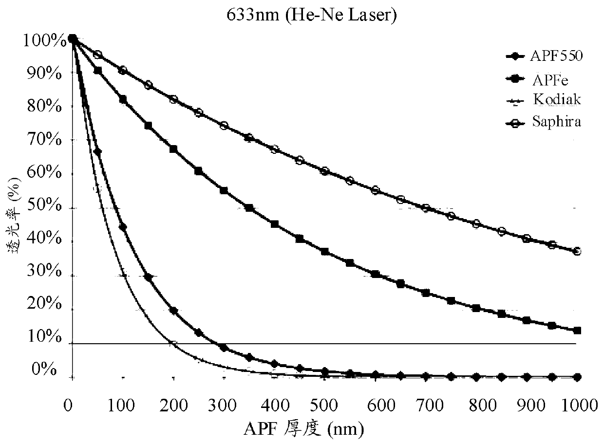
However, as the thickness and density of the material increase, the absorption of light by these layers increases, and the reflection decreases, which has a great impact on the photolithography process, especially the overlay (OVL, Overlay) after the photolithography process. The difficulty of measurement increases, and the OVL measurement accuracy of the developed graphics is relatively low, which affects the OVL compensation result and thus affects the final yield level

Method used


Image

  • Overlay marking method, overlay measuring method and overlay mark
  • Overlay marking method, overlay measuring method and overlay mark
  • Overlay marking method, overlay measuring method and overlay mark

Examples


Embodiment Construction

[0050] In order to make the technical solutions and advantages of the embodiments of the present application clearer, the specific technical solutions of the present application will be further described in detail below in conjunction with the drawings in the embodiments of the present application. The following examples are used to illustrate the present application, but not to limit the scope of the present application.

[0051] In the following description, references to "some embodiments" describe a subset of all possible embodiments, but it is understood that "some embodiments" may be the same subset or a different subset of all possible embodiments, and Can be combined with each other without conflict.

[0052] If there is a similar description of "first / second" in the application documents, add the following explanation. In the following description, the terms "first\second\third" are only used to distinguish similar objects, not Represents a specific ordering of objec...


PUM


Abstract

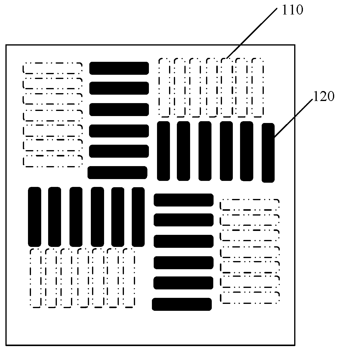
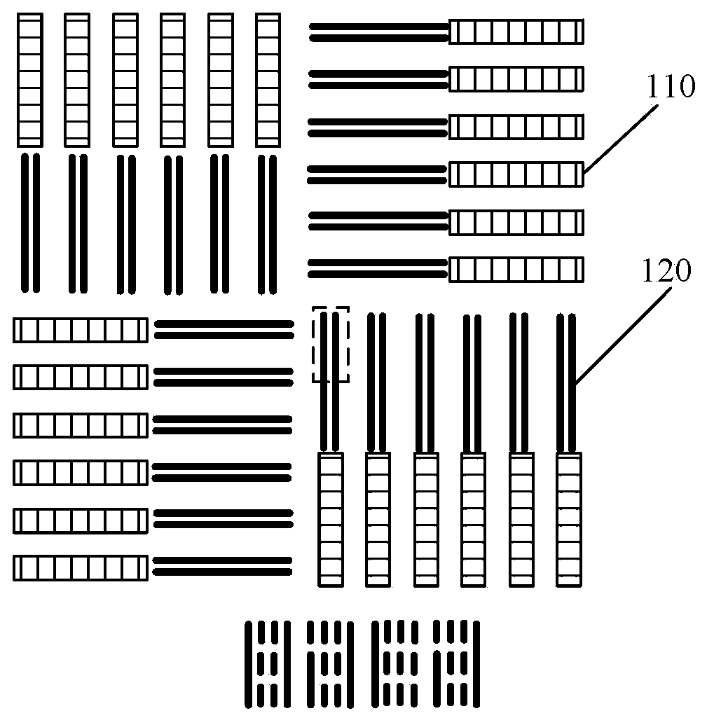
The embodiment of the invention discloses an overlay marking method, an overlay measuring method and an overlay mark. The overlay marking method comprises the steps of forming N first marks are formedon a first material layer, wherein each first mark comprises P first sub-marks, and each first sub-mark is in a long strip shape formed by a plurality of blocky patterns; forming a second material layer after the first material layer; forming n second marks in one-to-one correspondence with the first marks on the second material layer, wherein each second mark comprises Q long-strip-shaped secondsub-marks, N, P and Q are all integers greater than 1, P is greater than Q, and the width of the first mark is greater than that of the second mark.

Description

technical field [0001] The embodiments of the present application relate to the field of semiconductor devices and their manufacture, and relate to, but are not limited to, an overlay marking method, an overlay measuring method, and overlay marking. Background technique [0002] In the manufacturing process of three-dimensional flash memory (3D NAND), in order to meet the high aspect ratio and high selection ratio requirements of the gate line (GL) etching (Etch) process, it is necessary to use a thicker and denser hard mask (HM, hard mask) as a shape-preserving material. However, as the thickness and density of the material increase, the absorption of light by these layers increases, and the reflection decreases, which has a great impact on the photolithography process, especially the overlay (OVL, Overlay) after the photolithography process. Measurement difficulties increase, and the OVL measurement accuracy of the developed pattern is relatively low, which affects the OV...

Claims


Application Information

Patent Timeline
IPC IPC(8): H01L23/544H01L21/66
CPCG03F7/70633
Inventor 万浩卢绍祥李伟郭芳芳陆聪轩攀登
Owner YANGTZE MEMORY TECH CO LTD
Why Eureka
Try Eureka