Circuit board detection method

A detection method and circuit board technology, which is applied in the detection field, can solve the problems of circuit board deformation, film expansion and shrinkage improvement, and circuit board size is not exactly the same, so as to improve the service life and avoid the effect of expansion and contraction

Inactive Publication Date: 2021-05-14
C SUN MFG
View PDF4 Cites 0 Cited by
  • Summary
  • Abstract
  • Description
  • Claims
  • Application Information

AI Technical Summary

Problems solved by technology

In the existing circuit board production method, the exposure operation of the circuit board needs to be carried out with a negative film, but the circuit board is often deformed due to the error in the manufacturing process, and the size of each circuit board is not exactly the same.
Furthermore, when the circuit board is exposed to film, the most critical factor affecting the quality of the film is often the problem of expansion and contraction, and the expansion and contraction of the film is too frequent or the expansion and contraction of the film are too large, which will easily shorten the use of the film. life
However, in the existing circuit board production process, there is no corresponding improvement plan for the expansion and contraction of the film.

Method used


Image

  • Circuit board detection method
  • Circuit board detection method
  • Circuit board detection method

Examples


Embodiment 1

[0027] see Figure 1 to Figure 6 , is Embodiment 1 of the present invention. What needs to be explained first is that this embodiment corresponds to the relevant quantities and shapes mentioned in the drawings, and is only used to specifically illustrate the implementation of the present invention, so as to facilitate the understanding of the content of the present invention. , not to limit the protection scope of the present invention.

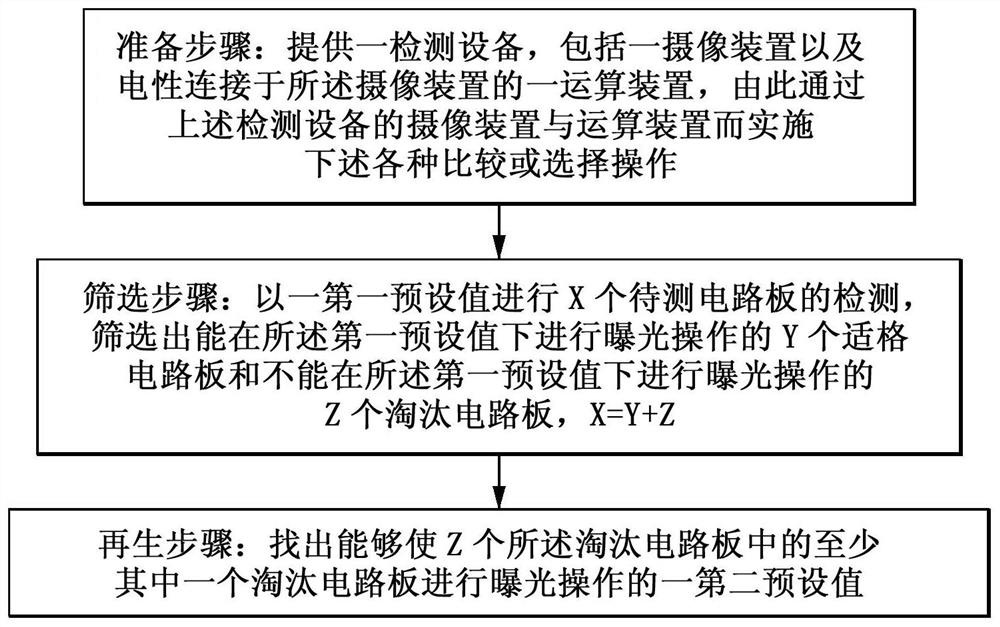
[0028] like figure 1 As shown, this embodiment discloses a circuit board inspection method, especially a circuit board inspection method before exposure operation. The circuit board inspection method includes the following steps: a preparation step, a screening step, a regeneration step, and an exposure step. The specific implementation of each step will be described below, but the following description does not limit the necessary implementation sequence of each step.

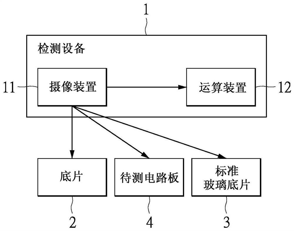
[0029] Preparation steps: see figure 2 and image 3 As shown, a de...

Embodiment 2

[0040] see Figure 7 , which is Embodiment 2 of the present invention. This embodiment is similar to Embodiment 1 above, and the same parts will not be described again. The main differences between the two embodiments are as follows.

[0041] Specifically, this embodiment discloses a circuit board exposure method, including the circuit board detection method described in Embodiment 1 and an exposure step. Wherein, the exposing step is: according to the first preset value R1, sequentially exposing the Y qualified circuit boards 41, and exposing at least one of the corresponding circuit boards 41 according to the second preset value R2. The exposing operation is performed on the elimination circuit board 42 described above.

[0042] Furthermore, according to the above-mentioned M kinds of preset values, the corresponding elimination circuit boards 42 are respectively subjected to an exposure operation. It should be noted that if the number of eliminated circuit boards 42 corre...

Embodiment 3

[0044] see Figure 8 and Figure 9 , is Embodiment 3 of the present invention. This embodiment is similar to the above-mentioned Embodiment 2, and the similarities will not be described again. The main differences between this embodiment and the above-mentioned two embodiments are as follows.

[0045] Specifically, this embodiment discloses a circuit board inspection method, which includes a preparation step, a screening step, a regeneration step, and an exposure step, so the circuit board inspection method in this embodiment can also be called a circuit board inspection method. method (or circuit board exposure method). Among them, the above-mentioned preparation steps, screening steps, regeneration steps, and exposure steps have been described in the first and second embodiments and will not be repeated in this embodiment, and this embodiment will further explain how to improve the exposure steps in the following .

[0046] Further, the exposure step is implemented in an ...


PUM


Abstract

The invention discloses a circuit board detection method. The circuit board detection method includes: a screening step, a regeneration step and an exposure step; A qualified circuit board for exposure operation under the first preset value, and an eliminated circuit board that cannot perform exposure operation under the first preset value; A second preset value, and the second preset value is relative to a second film; the exposure step is implemented in an exposure device, and an environment in the exposure device is controlled by an environment control structure The temperature is cooled, so that the Y qualified circuit boards, the first negative, the at least one eliminated circuit board, and the second negative can be maintained during the exposure operation in the exposure equipment. The ambient temperature is below a predetermined temperature.

Description

technical field [0001] The invention relates to a detection method, in particular to a circuit board detection method. Background technique [0002] Today's advanced technology has led to the development of various electronic products, and various electronic products mostly use printed circuit boards as their basic components. Therefore, providing high-quality printed circuit boards is the development direction that various manufacturers want to pursue. In the existing circuit board production method, the exposure operation of the circuit board needs to be carried out with a negative film, but the circuit board is often deformed due to the error in the manufacturing process, and the size of each circuit board is not exactly the same. Furthermore, when the circuit board is exposed to film, the most critical factor affecting the quality of the film is often the problem of expansion and contraction, and the expansion and contraction of the film is too frequent or the expansion ...

Claims


Application Information

Patent Timeline
Patent Type & Authority Patents(China)
IPC IPC(8): H05K3/00
CPCH05K3/00
Inventor 王启毓郑章民
Owner C SUN MFG
Why Eureka
Try Eureka