Packaging structure of scanning micromirror

A scanning micromirror and packaging structure technology, applied in the field of spectrometers, can solve the problems of easy damage to the lower printed circuit board circuit, increasing the driving voltage of the scanning micromirror chip, unsuitable for mass production of products, etc. Mass production, simple and stable packaging structure, and small distance

Active Publication Date: 2022-07-12
CHONGQING CHUANYI AUTOMATION
View PDF6 Cites 0 Cited by
  • Summary
  • Abstract
  • Description
  • Claims
  • Application Information

AI Technical Summary

Problems solved by technology

This packaging structure is complex and unstable, and there are many packaging steps, which reduces the processing efficiency
The connection between the upper printed circuit board, the micromirror holder and the lower printed circuit board is also unstable, and the consistency of the packaging is also poor, which is not suitable for mass production of products
Moreover, the lower printed circuit board is exposed, and the lower printed circuit board is not protected. After long-term use, the lines in the lower printed circuit board are easily damaged, which affects the normal operation of the spectrometer
Simultaneously, two magnets are located at the two ends of the upper printed circuit board, and the distance between the magnet and the micromirror chip is far, and the situation of insufficient magnetic force will occur, thus increasing the driving voltage of the scanning micromirror chip and increasing the external circuit load

Method used


Image

  • Packaging structure of scanning micromirror
  • Packaging structure of scanning micromirror
  • Packaging structure of scanning micromirror

Examples


Embodiment Construction

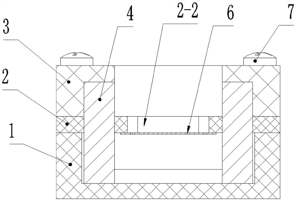
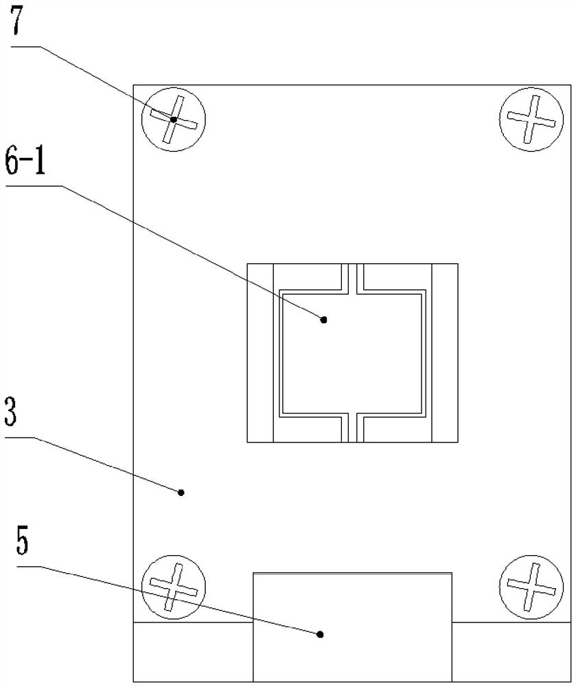
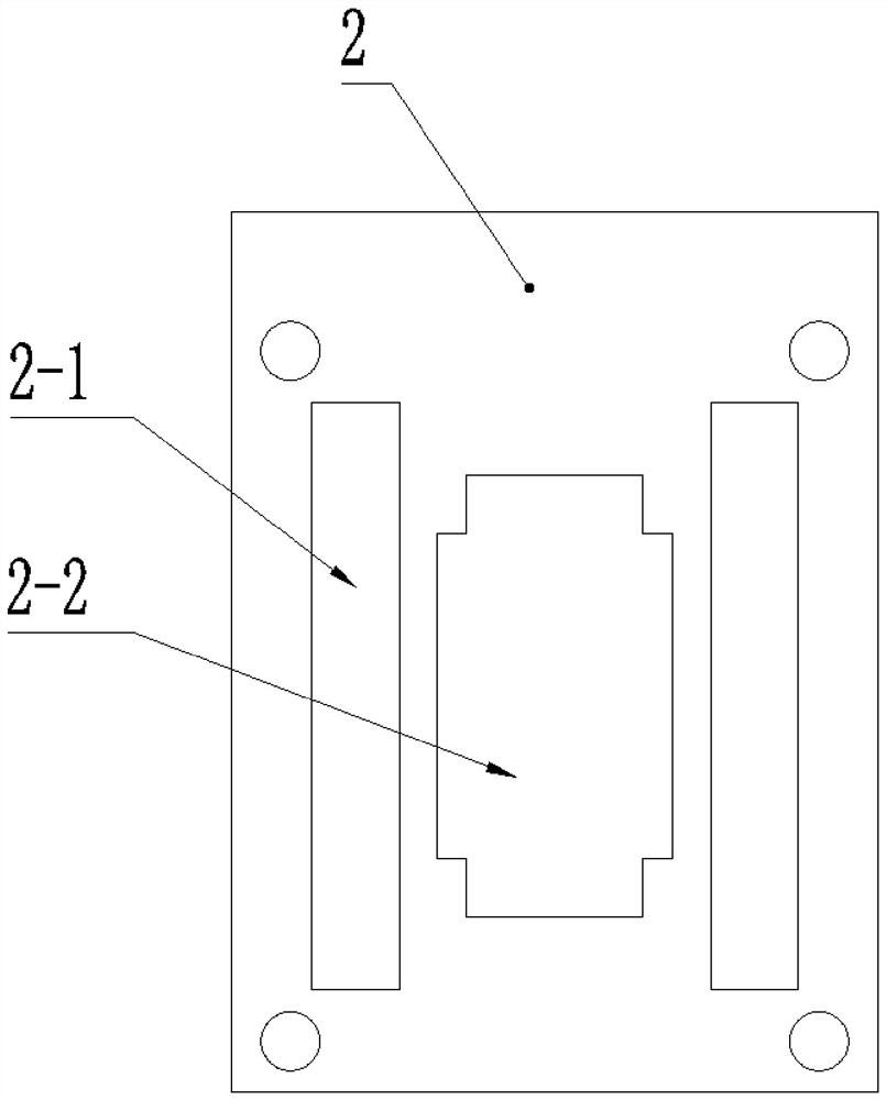
[0033] see Figure 1 to Figure 10, an encapsulation structure of a scanning micromirror, comprising a base 1 , a cavity 1 - 1 is arranged on the upper end of the base 1 , and a printed circuit board 2 is placed on the upper end of the base 1 . The middle of the printed circuit board 2 is provided with a via hole 2-2 for light to pass through, and two mounting holes 2-1 are symmetrically arranged on the left and right sides of the via hole 2-2 on the printed circuit board 2. Magnets 4 are respectively fixed in the mounting holes 2-1. The front and rear cavity walls of the cavity 1-1 of the base 1 are provided with a limit protrusion 1-2, and the left and right ends of each limit protrusion 1-2 are connected to the left and right cavity walls of the cavity 1-1. There are gaps 1-3 between them, and the lower ends of the magnets 4 in the two mounting holes 2-1 are inserted into the gaps 1-3 respectively and abut against the bottom of the cavity 1-1 of the base 1 . The fixing of ...


PUM


Abstract

The invention relates to an encapsulation structure of a scanning micromirror, comprising a base, the upper end of the base is provided with a concave cavity, a printed circuit board is placed on the upper end of the base, and the middle of the printed circuit board is provided with a via hole for light to pass through, so the Two mounting holes are symmetrically arranged on the left and right sides of the via holes on the printed circuit board, magnets are respectively fixed in the mounting holes, the lower ends of the magnets are pressed against the bottom of the cavity of the base, and a scanning micromirror chip is fixed on the bottom of the cavity. The lower end face of the printed circuit board, the mirror surface of the scanning micromirror chip is located below the through hole of the printed circuit board, the upper end of the printed circuit board is provided with a cable terminal, and one end is covered on the printed circuit board. On the upper end, the printed circuit board and the magnet are pressed, and the end cover, the printed circuit board and the base are fixed together by bolts. The structure is simple and stable, the packaging is simple and fast, the packaging consistency is good, and the positioning of the two magnets is good.

Description

technical field [0001] The invention relates to the technical field of spectrometers, in particular to a packaging structure of a scanning micromirror. Background technique [0002] The scanning micromirror is used in the infrared spectrometer, so that the single-tube detector replaces the traditional expensive array detector. The scanning micromirror is small in size and low in cost, which can reduce the size of the spectrometer. The current scanning micromirror uses two upper and lower printed circuit boards, the lower printed circuit board is fixed on the lower end of the micromirror seat, the scanning micromirror chip is fixed on the upper printed circuit board, the upper printed circuit board, the micromirror The seat and the lower printed circuit board are passed through the pin headers in sequence and then fixed together by soldering. Two magnets are installed on the micro-mirror holder, and the two magnets are respectively located on the left and right sides of the ...

Claims


Application Information

Patent Timeline
Patent Type & Authority Patents(China)
IPC IPC(8): H05K1/18H05K7/14
CPCH05K1/18H05K7/14
Inventor 吴轲黄明洋周颖黄云彪
Owner CHONGQING CHUANYI AUTOMATION
Why Eureka
Try Eureka