
Display panel and preparation method thereof

A display panel and display area technology, applied in semiconductor/solid-state device manufacturing, instruments, semiconductor devices, etc., can solve problems such as occupation, large screen space, no front flash, etc., to achieve controllability, reduce power consumption, The effect of reducing the brightness of the light

Active Publication Date: 2020-06-02
TCL CHINA STAR OPTOELECTRONICS TECH CO LTD
View PDF5 Cites 1 Cited by
  • Summary
  • Abstract
  • Description
  • Claims
  • Application Information

AI Technical Summary

Problems solved by technology

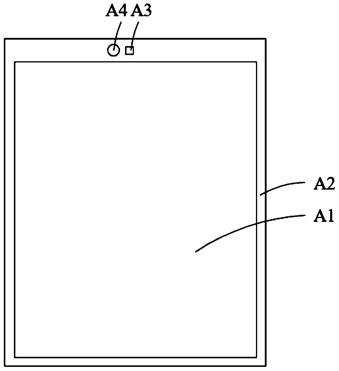
[0002] With the gradual popularity of full-screen and narrow-frame display devices, it is particularly important to rationalize the space of the display screen. If the front flash uses an external flash, it will take up a large screen space, resulting in most full-screen display devices. No front flash function

Method used


Image

  • Display panel and preparation method thereof
  • Display panel and preparation method thereof
  • Display panel and preparation method thereof

Examples


Embodiment Construction

[0028] The following will clearly and completely describe the technical solutions in the embodiments of the present invention with reference to the accompanying drawings in the embodiments of the present invention. Obviously, the described embodiments are only some, not all, embodiments of the present invention. Based on the embodiments of the present invention, all other embodiments obtained by those skilled in the art without creative efforts fall within the protection scope of the present invention.

[0029] In describing the present invention, it should be understood that the terms "center", "longitudinal", "transverse", "length", "width", "thickness", "upper", "lower", "front", " The orientation or positional relationship indicated by "rear", "left", "right", "vertical", "horizontal", "top", "bottom", "inner", "outer", etc. is based on the orientation shown in the drawings Or positional relationship is only for the convenience of describing the present invention and simpl...


PUM


Abstract

The invention discloses a display panel and a preparation method thereof. The display panel comprises an array substrate, and the array substrate comprises a display area and a non-display area; a plurality of display area thin film transistors arranged in an array are configured on the array substrate; and the non-display area is arranged it the periphery of the display area, and comprises a flash lamp area; and the flash lamp area is configured with at least one flash lamp area thin film transistor, at least one external electrode corresponding to the at least one flash lamp area thin film transistor, and at least one light emitting diode electrically connected with the at least one flash lamp area thin film transistor and the at least one external electrode. According to the display panel, the flash lamp can be arranged in the display panel, so that the display panel has richer functions and market competitiveness.

Description

technical field [0001] The present application relates to the field of display technology, in particular to a display panel and a manufacturing method thereof. Background technique [0002] With the gradual popularity of full-screen and narrow-frame display devices, it is particularly important to rationalize the space of the display screen. If the front flash uses an external flash, it will take up a large screen space, resulting in most full-screen display devices. No front flash function. [0003] In view of the higher and higher requirements of users for the camera or photography function of display devices, the demand for more front flashes, ambient light compensation and space optimization of flashes for full-screen display devices is becoming more and more important. Contents of the invention [0004] In order to solve the above problems, in the first aspect, the present invention provides a display panel, which includes: an array substrate, in the display area, th...

Claims


Application Information

Patent Timeline
IPC IPC(8): H01L27/32H01L27/12H01L51/52H01L51/56G02F1/1362G02F1/1343
CPCH01L27/1214G02F1/1362G02F1/134309H10K59/00H10K50/84H10K71/00
Inventor 周万亮
Owner TCL CHINA STAR OPTOELECTRONICS TECH CO LTD
Learn More