A display panel, its driving method and display device

A display panel and substrate substrate technology, applied in the direction of static indicators, instruments, electric solid devices, etc., can solve problems such as lateral crosstalk, affecting pixel light emission, and poor display effect of the display panel, so as to avoid lateral crosstalk and improve display effect , Reduce the effect of lateral conductivity

Active Publication Date: 2022-08-09
BOE TECH GRP CO LTD
View PDF5 Cites 0 Cited by
  • Summary
  • Abstract
  • Description
  • Claims
  • Application Information

AI Technical Summary

Problems solved by technology

However, in the manufacturing process of the white organic light-emitting unit, the internal organic layers, such as the hole injection layer (Hole Injection HIL, HIL), the hole transport layer (Hole Transport Layer, HTL), the electron transport layer (Electron Transport Layer) , ETL)) and the light-emitting layer (Emission Layer, EL), if there are more carriers in an organic layer, the carriers will inevitably move laterally along the organic layer, resulting in enhanced lateral conductivity of the organic layer , for example, when there is current in a pixel, the organic layer with strong lateral conductivity conducts carriers to adjacent pixels, thereby affecting the light emission of adjacent pixels
[0004] It can be seen that the prior art has the technical problems of lateral crosstalk and poor display effect of the display panel

Method used


Image

  • A display panel, its driving method and display device
  • A display panel, its driving method and display device
  • A display panel, its driving method and display device

Examples


Embodiment Construction

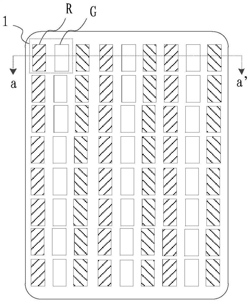
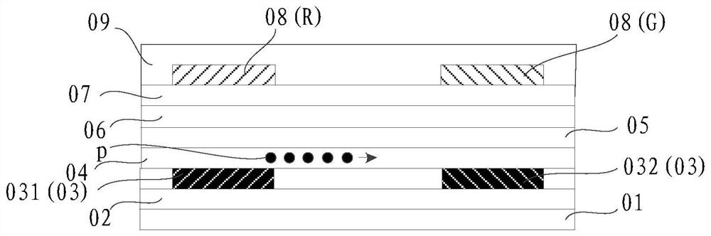
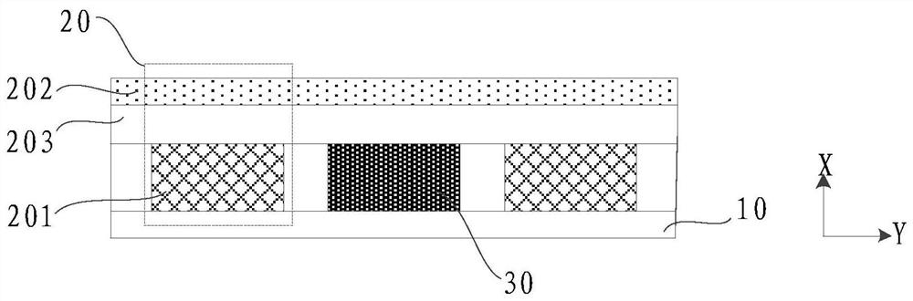
[0036] In order to make the purpose, technical solutions and advantages of the embodiments of the present invention clearer, the technical solutions of the embodiments of the present invention will be clearly and completely described below with reference to the accompanying drawings of the embodiments of the present invention. Obviously, the described embodiments are some, but not all, embodiments of the present invention. Also, the embodiments of the present invention and the features of the embodiments may be combined with each other without conflict. Based on the described embodiments of the present invention, all other embodiments obtained by those of ordinary skill in the art without creative work fall within the protection scope of the present invention.

[0037] Unless otherwise defined, technical or scientific terms used in the present invention should have the ordinary meaning as understood by one of ordinary skill in the art to which the present invention belongs. T...


PUM


Abstract

The present invention provides a display panel, a driving method thereof, and a display device, wherein the display panel includes: a base substrate, and a plurality of light-emitting units arranged in an array on the base substrate; Any one of the light-emitting units includes an anode, a cathode, and a light-emitting functional layer disposed between the anode and the cathode, wherein a preset distance is spaced between two adjacent anodes; the blocking structure is disposed at the between the light-emitting functional layer and the base substrate, and at least partially between two adjacent anodes, wherein the orthographic projection of the blocking structure on the base substrate is the same as the anode on the The orthographic projections on the base substrate do not overlap each other; wherein, the blocking structure receives electrical signals to generate an electric field in a direction perpendicular to the plane of the base substrate. It is used to solve the technical problem of lateral crosstalk and improve the display effect of the display panel.

Description

technical field [0001] The present invention relates to the field of display technology, and in particular, to a display panel, a driving method thereof and a display device. Background technique [0002] The organic light emitting diode (Organic Light Emitting Display, OLED) display panel has attracted extensive attention due to its advantages of self-luminescence, fast response, wide viewing angle, high brightness, bright color, and thinness. [0003] For a silicon-based OLED display panel, a white organic light-emitting unit and a color filter layer are usually used to realize the light emission of red pixels, green pixels and blue pixels. However, in the production process of the white organic light-emitting unit, the internal organic layers, such as the hole injection layer (Hole Injection HIL, HIL), the hole transport layer (Hole Transport Layer, HTL), the electron transport layer (Electron Transport Layer) , ETL)) and the emission layer (Emission Layer, EL), if there...

Claims


Application Information

Patent Timeline
Patent Type & Authority Patents(China)
IPC IPC(8): H01L51/50H01L51/52H01L27/32G09G3/3208
CPCG09G3/3208H10K59/00H10K50/125H10K50/81H10K59/35H10K50/818H10K2102/3026H10K59/353H10K59/131
Inventor 岳晗张粲玄明花陈小川
Owner BOE TECH GRP CO LTD
Why Eureka
Try Eureka