Supercharge Your Innovation With Domain-Expert AI Agents!

Radio frequency copper detector and automatic correction system and detection method and automatic correction method

A radio frequency and automatic technology, applied in the field of etching process and etching process system, can solve the problems of inaccurate detection results, inaccurate results, waste of resources and costs, etc.

Active Publication Date: 2020-06-23
AMPOC FAR EAST CO LTD
View PDF6 Cites 0 Cited by
  • Summary
  • Abstract
  • Description
  • Claims
  • Application Information

AI Technical Summary

Problems solved by technology

[0005] However, this method is quite time-consuming, so it can only be sampled and cannot detect all the substrates 92, so that the obtained results are relatively inaccurate
and, if Figure 8 As shown, the detection by the contact sensor 91 can only arrange the detection points 921 on the substrate 92 as much as possible, but cannot reliably detect all the surfaces of the substrate 92, resulting in the generation of undetected gaps 922, which will also cause make test results less accurate
The above two shortcomings will lead to a decline in the yield of the entire etching process
[0006] In addition, after the inspection of the substrate 92, if the copper plating thickness and the uniformity of the copper plating thickness do not meet the acceptable error range of the etching process, they will be eliminated in batches, which is quite a waste of resources and costs.

Method used


Image

  • Radio frequency copper detector and automatic correction system and detection method and automatic correction method
  • Radio frequency copper detector and automatic correction system and detection method and automatic correction method
  • Radio frequency copper detector and automatic correction system and detection method and automatic correction method

Examples


Embodiment Construction

[0046] The technical means adopted by the present invention to achieve the intended creation purpose are further described below in conjunction with the accompanying drawings and preferred embodiments of the present invention.

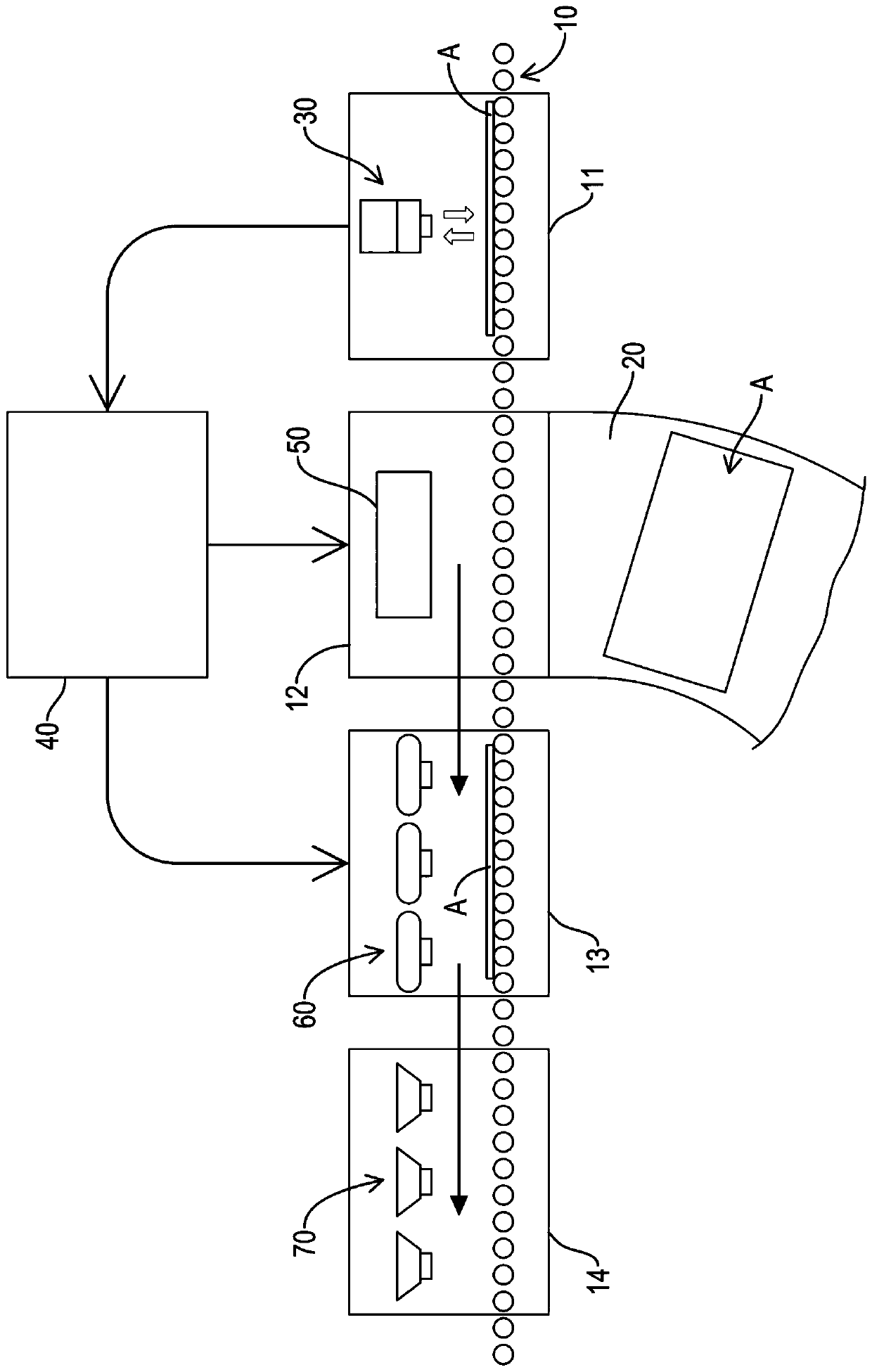
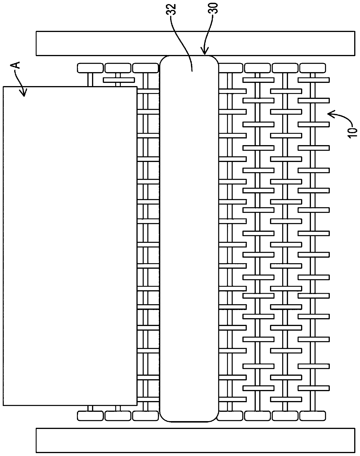
[0047] see figure 1 and figure 2 As shown, the substrate thickness detection and automatic correction system of the present invention is used to detect and correct the thickness of the copper plating on the surface of a substrate A or the uniformity of the copper plating thickness on the surface. The substrate thickness detection and automatic correction system includes a transport track 10 , a removal track 20 , a radio frequency copper measuring instrument 30 , a computing unit 40 , a removal device 50 , a pre-etching device 60 and a main etching device 70 .

[0048] The conveying track 10 includes a detection area 11 , a discrimination area 12 , a correction area 13 and an etching area 14 which are sequentially connected. The transport track 10 ...


PUM


Abstract

The invention relates to an etching process system and method. The etching process system comprises a radio frequency copper detector and a pre-etching device. The radio frequency copper detector comprises a plurality of sensors, each sensor can emit and receive radio frequency, and radio frequency covering ranges of the multiple sensors overlap one another and are sufficient to stretch across the two ends of a substrate for etching. After scanning the substrate, the radio frequency copper detector transmits data to the pre-etching device for compensating spraying, so as to correct the abnormal thickness and uniformity. Therefore, according to the etching process system and method, all surfaces of each substrate can be scanned one by one and completely, and the obtained thicknesses of thesurface copper plating or the uniformity of the surface copper plating thickness is very accurate, and the detection time required is short, and after the data is obtained, pre-etching can be carriedout immediately for correction, and thus the waste of resources and costs is greatly reduced.

Description

technical field [0001] The invention relates to an etching process system and an etching process method. Background technique [0002] The etching process is one of the commonly used processes in the modern high-tech industry to manufacture electronic components such as chips. Etching generally works by engraving desired shapes on the surface of a substrate using physical or chemical reactions. Generally speaking, the aforementioned substrate is usually a multilayer board with copper foil plated on its surface, while the etching process in the prior art is to spray a chemical solvent corrosive to the copper foil on the surface of the copper foil to achieve the purpose of etching. Therefore, the thickness of the copper foil plated on the surface of the substrate and the uniformity of the thickness of the copper foil become important factors affecting the yield of the etching process. [0003] Therefore, in the prior art, the operator of the etching process must first measur...

Claims


Application Information

Patent Timeline
Patent Type & Authority Applications(China)
IPC IPC(8): C23F1/08C23F1/02G01B7/06
CPCC23F1/08C23F1/02G01B7/066
Inventor 苏胜義乔鸿培吕理榕巫坤星
Owner AMPOC FAR EAST CO LTD
Features
  • R&D
  • Intellectual Property
  • Life Sciences
  • Materials
  • Tech Scout
  • Unparalleled Data Quality
  • Higher Quality Content
  • 60% Fewer Hallucinations
Learn More