
Filter circuit and filtering method thereof

A filter circuit and capacitor technology, which is applied in the field of integrated circuit design, can solve problems such as high cost, high failure risk, and complex peripheral circuits of the chip, and achieve the effect of reducing capacitance, simplifying the peripheral circuit of the chip, and reducing the risk of failure

Active Publication Date: 2020-06-23
CRM ICBG (WUXI) CO LTD
View PDF3 Cites 1 Cited by
  • Summary
  • Abstract
  • Description
  • Claims
  • Application Information

AI Technical Summary

Problems solved by technology

[0005] In view of the shortcomings of the prior art described above, the purpose of the present invention is to provide a filter circuit and a filter method thereof, which are used to solve the problem of complex peripheral circuits, high cost, and failure risks of the chip peripheral circuit of the duty ratio signal filter circuit in the prior art. advanced questions

Method used


Image

  • Filter circuit and filtering method thereof
  • Filter circuit and filtering method thereof
  • Filter circuit and filtering method thereof

Examples


Embodiment 1

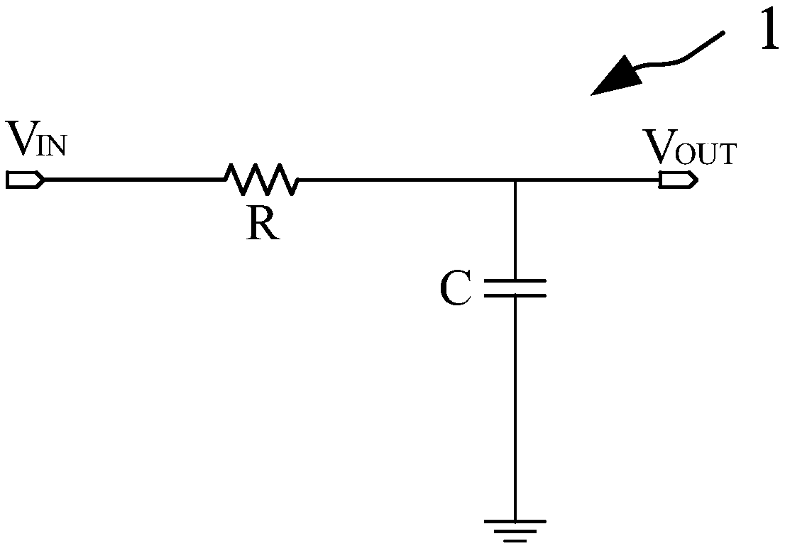
[0036] Such as figure 1 As shown, this embodiment provides a filter circuit 1, the filter circuit includes:

[0037] Resistor R and filter capacitor C.

[0038] Such as figure 1 As shown, the input terminal of the resistor R receives the input signal V IN , the output terminal outputs the signal V OUT ; The upper plate of the filter capacitor C is connected to the output end of the resistor R, and the lower plate is grounded.

[0039] It should be noted that, in this embodiment, the resistor R is set inside the chip, and the filter capacitor C is set outside the chip.

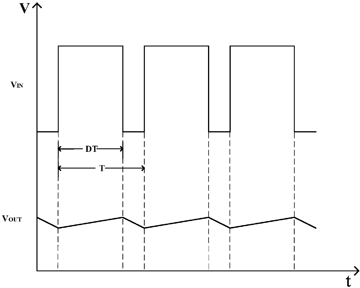
[0040] Specifically, in this embodiment, the input signal V IN It is a power frequency duty ratio square wave signal, the resistor R inside the chip and the filter capacitor C outside the chip form a first-order low-pass filter, which can filter out the high frequency components of the power frequency duty ratio square wave signal , and then perform filtering processing on the power frequency duty ratio s...

Embodiment 2

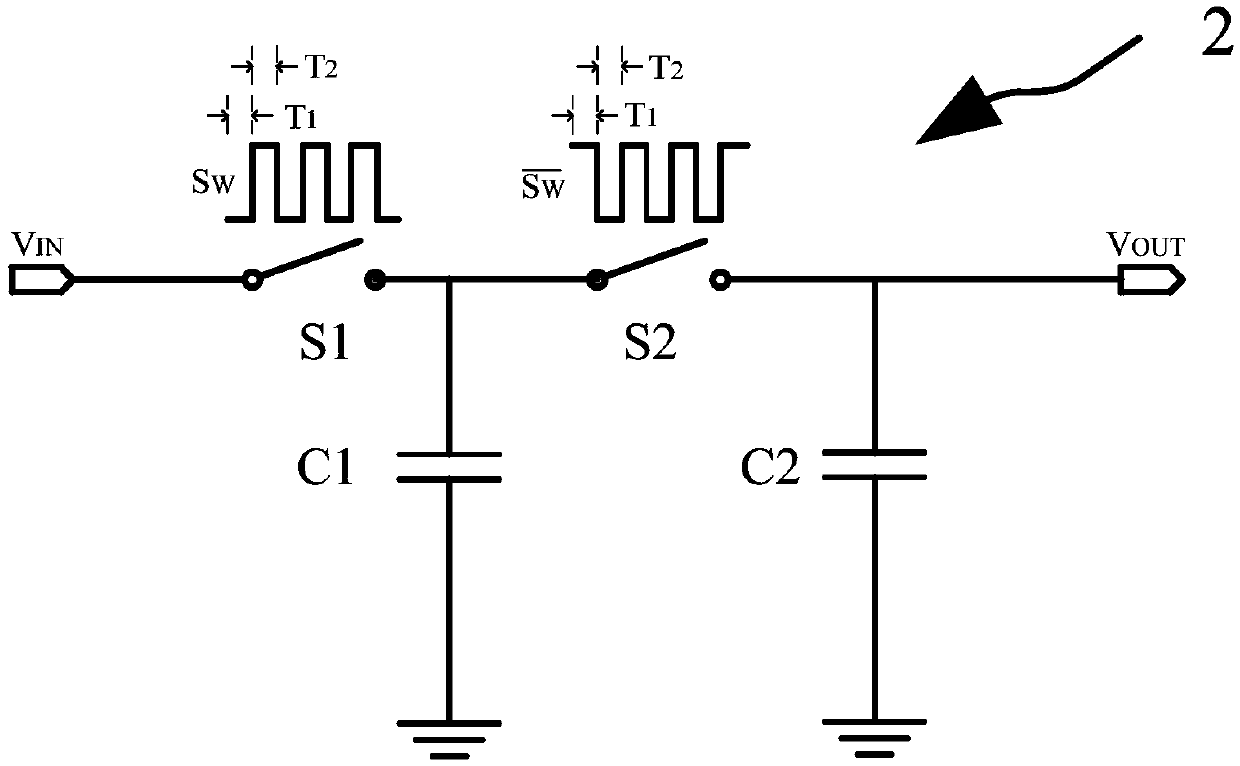
[0054] Such as image 3 As shown, this embodiment provides a filter circuit 2, and the filter circuit 2 includes:

[0055] The first switch S1, the second switch S2, the first capacitor C1 and the second capacitor C2.

[0056] Such as image 3As shown, one end of the first switch S1 is connected to the input signal V IN , the other end is connected to the upper plate of the first capacitor C1, and the lower plate of the first capacitor C1 is grounded. One end of the second switch S2 is connected to the upper plate of the first capacitor C1, the other end is connected to the upper plate of the second capacitor C2, and the lower plate of the second capacitor C2 is grounded. The upper plate of the second capacitor C2 is used as an output terminal.

[0057] Specifically, the first switch S1 includes, but is not limited to, an insulated gate bipolar transistor or a metal-oxide semiconductor field effect transistor. Any device that can realize a switching function is applicable ...


PUM


Abstract

The invention provides a filter circuit and a filtering method thereof. The filter circuit comprises a first switch and a second switch, wherein one end of the first switch is connected with an inputsignal, the other end of the first switch is connected with an upper pole plate of a first capacitor, and a lower pole plate of the first capacitor is grounded; one end of the second switch is connected with the upper pole plate of the first capacitor, the other end of the second switch is connected with an upper pole plate of a second capacitor, and a lower pole plate of the second capacitor is grounded; and the switching signal of the first switch and the switching signal of the second switch are opposite in phase. When the first switch is turned on, an input signal charges and discharges the first capacitor, the second switch is turned off, the voltage on the second capacitor is not changed, and stable output is realized; when the first switch is turned off, the input signal is disconnected with the first capacitor, the second switch is turned on, the first capacitor charges and discharges the second capacitor, and the output signal changes along with the voltage of the second capacitor. The filter circuit is simple in structure and higher in integration level, the configuration of a large filter capacitor can be omitted, a peripheral circuit is simplified, the system cost is reduced, and the failure problem caused by the peripheral filter capacitor is thoroughly eliminated.

Description

technical field [0001] The invention relates to the field of integrated circuit design, in particular to a filter circuit and a filter method thereof. Background technique [0002] With the continuous upgrading of LED drive circuits, the simplification of peripheral circuits, the low cost of the overall solution, and high reliability have become the direction and goal that everyone has unanimously recognized. In the LED drive circuit, it is often necessary to filter the power frequency duty cycle square wave signal to obtain a voltage reference that can reflect the duty cycle, and then proceed to the next step according to the voltage reference. For example, in the LED thyristor dimming circuit, it is necessary to cut off the phase angle of the bus voltage of the thyristor, first convert it into a duty ratio square wave signal, and then convert it into a voltage reference of the corresponding size, and finally control the level of the voltage reference The brightness of the...

Claims


Application Information

Patent Timeline
IPC IPC(8): H02M1/15
CPCH02M1/15
Inventor 张识博卢圣晟李亮
Owner CRM ICBG (WUXI) CO LTD
Learn More