Semiconductor cleaning device with on-line monitoring function

A cleaning device and monitoring device technology, which is applied in semiconductor/solid-state device manufacturing, electrical components, circuits, etc., can solve problems such as poor detection ability, and achieve the effect of improving production efficiency and yield

Pending Publication Date: 2020-07-03
WUHAN UNIV
View PDF5 Cites 0 Cited by
  • Summary
  • Abstract
  • Description
  • Claims
  • Application Information

AI Technical Summary

Problems solved by technology

However, it mainly focuses on the detection of a single aspect, and the detection ability is poor, and the material cleaning process involves the evolution of the material microstructure, the stress change of the material, etc.
At present, there is a lack of using a variety of more advanced measurement methods to detect these microscopic changes in order to explore the process of material cleaning in essence, so as to optimize the material cleaning process more scientifically and determine the best cleaning process for different materials.

Method used


Image

  • Semiconductor cleaning device with on-line monitoring function

Examples


Embodiment Construction

[0020] The following will clearly and completely describe the technical solutions in the embodiments of the present invention with reference to the accompanying drawings in the embodiments of the present invention. Obviously, the described embodiments are only some, not all, embodiments of the present invention. Based on the embodiments of the present invention, all other embodiments obtained by persons of ordinary skill in the art without creative efforts fall within the protection scope of the present invention.

[0021] It should be noted that, in the case of no conflict, the embodiments of the present invention and the features in the embodiments can be combined with each other.

[0022] The present invention will be further described below in conjunction with the accompanying drawings and specific embodiments, but not as a limitation of the present invention.

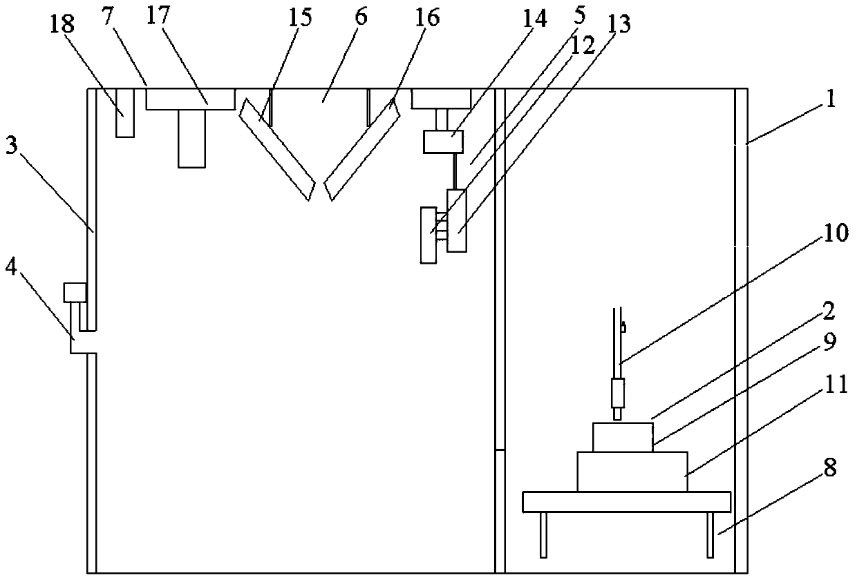
[0023] figure 1 It is a schematic structural diagram of a semiconductor cleaning device provided in an embodime...


PUM


Abstract

The invention relates to a semiconductor cleaning device with an online monitoring function. The semiconductor cleaning device comprises a cleaning chamber, a cleaning device for cleaning an etched array substrate, a monitoring chamber, an air extractor, a first monitoring device for monitoring the appearance and the surface roughness of the cleaned array substrate, a second monitoring device formonitoring the crystal phase change of the surface of the cleaned array substrate, a third monitoring device for monitoring the warping change of the surface of the cleaned array substrate, and a conveying device, wherein the cleaning device and the monitoring chamber are sequentially communicated with an etching cavity, the gas inlet of the air extractor is communicated with the monitoring chamber, the first monitoring device and the second monitoring device are arranged on the monitoring chamber, and the third monitoring device is arranged in the monitoring chamber. According to the semiconductor cleaning device provided by the invention, the cleaned array substrate is monitored by utilizing the corresponding monitoring device, so that parameters such as crystalline phase components, surface roughness and the like are obtained on line, the cleaning process is fed back and adjusted, and the production efficiency and the yield are further improved.

Description

technical field [0001] The invention relates to the technical field of process monitoring, in particular to a semiconductor cleaning device with an online monitoring function. Background technique [0002] Whether it is integrated circuits, advanced packaging, semiconductor lighting devices or power electronic devices, their performance is highly dependent on the quality control of the semiconductor material cleaning process. [0003] In the cleaning process of semiconductor materials, in order to meet the requirements of uniformity, high efficiency, low damage, low residue, and no re-oxidation of the cleaning materials, in the process of material cleaning, it is necessary to control the reaction temperature in the cleaning tank, the warpage of the material after cleaning, Real-time and precise control of index parameters that have a direct impact on material properties, such as cleaning speed, cleaning liquid flow, cleaning impact pressure, and cleaning device temperature. ...

Claims


Application Information

Patent Timeline
Patent Type & Authority Applications(China)
IPC IPC(8): H01L21/67
CPCH01L21/6708H01L21/67242H01L21/67288
Inventor 刘胜李瑞东芳王诗兆韩旭阳学进
Owner WUHAN UNIV
Why Eureka
Try Eureka