
Three-dimensional flash memory and manufacturing method thereof

A manufacturing method and technology of flash memory, applied in the field of memory, can solve problems such as limited integration and achieve the effect of reducing requirements

Active Publication Date: 2020-07-03
INST OF MICROELECTRONICS CHINESE ACAD OF SCI
View PDF11 Cites 0 Cited by
  • Summary
  • Abstract
  • Description
  • Claims
  • Application Information

AI Technical Summary

Problems solved by technology

However, limited by the current process conditions, even if expensive process equipment is continuously used to improve the precision of lithography and mask processes, the improvement of its integration level is still limited

Method used


Image

  • Three-dimensional flash memory and manufacturing method thereof
  • Three-dimensional flash memory and manufacturing method thereof
  • Three-dimensional flash memory and manufacturing method thereof

Examples


Embodiment Construction

[0047] The following will clearly and completely describe the embodiments of the present application with reference to the accompanying drawings in the embodiments of the present application. Obviously, the described embodiments are only some of the embodiments of the present application, not all of them. Based on the embodiments in this application, all other embodiments obtained by persons of ordinary skill in the art without making creative efforts belong to the scope of protection of this application.

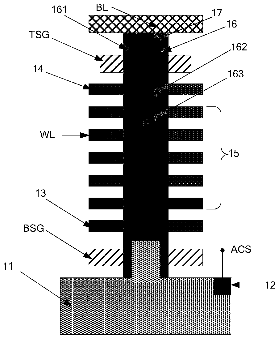
[0048] Such as figure 1 as shown, figure 1 It is a structural diagram of a 3D NAND with a conventional structure, including: a P-type well region 11, a storage stack structure disposed on the P-type well region 11, and an N-type doped region 12 disposed in the P-type well region 11, N The N-type doped region 12 is n+ doped, that is, the N-type heavily doped region. The storage stack structure includes: a lower selection transistor BSG, an upper selection transistor TSG, a...


PUM


Abstract

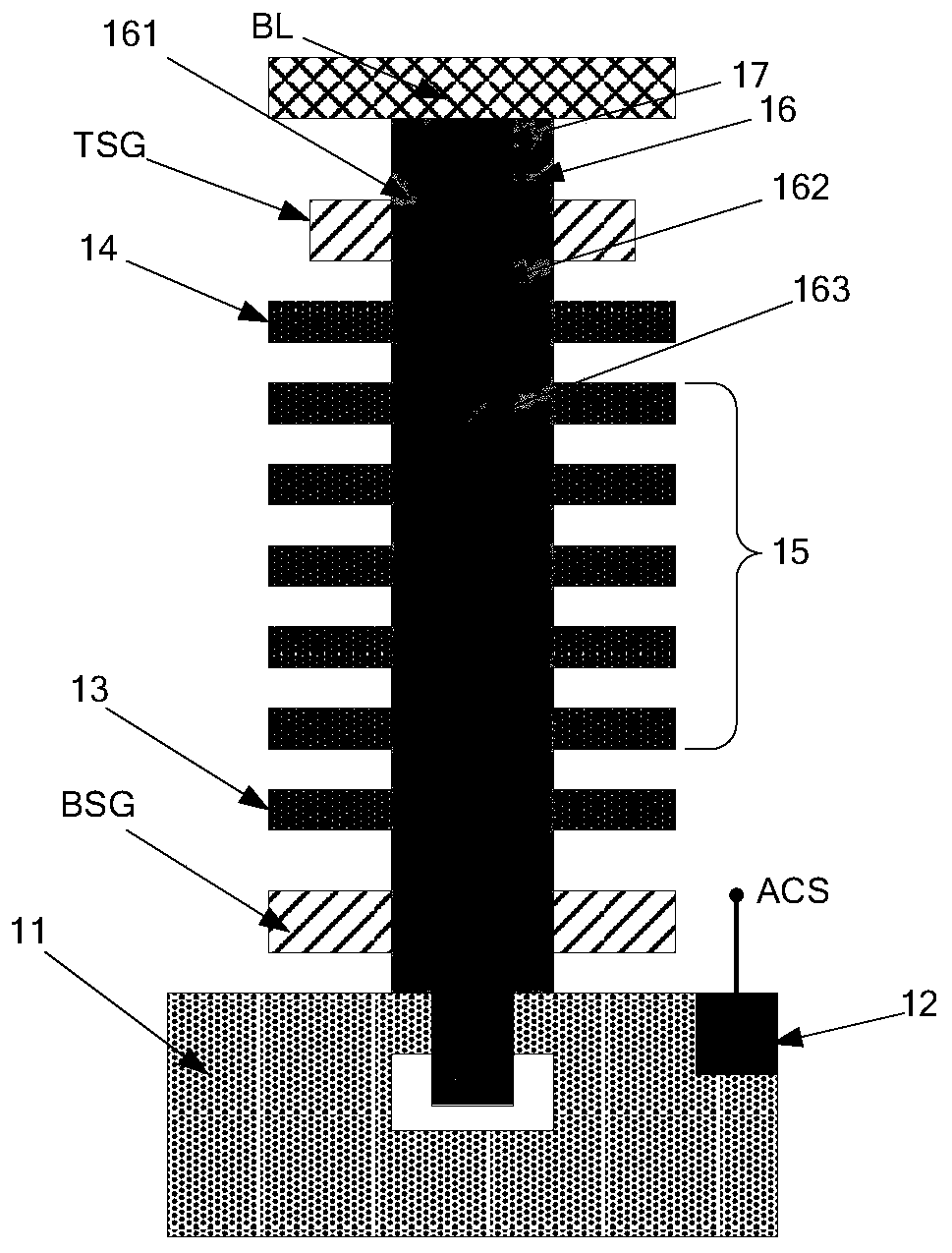
The invention discloses a three-dimensional flash memory and a manufacturing method thereof. According to the technical scheme of the invention, the side wall channel structure is arranged between thestorage stack structure and the substrate. The side wall channel structure comprises a second N-type doped layer and a P-type doped layer. The second N-type doped layer is located between the first N-type doped layer and the P-type doped layer. The P-type doped layer is used for connecting a P-type well region in the substrate during erasing operation and providing holes. The second N-type dopedlayer is used for providing a conductive channel during reading operation and providing electrons during programming operation, and independent transmission of electrons and holes can be realized. Inthe reading operation process, the electrons are transmitted through the second N-type doped layer at the middle upper part of the side wall channel structure, so that the requirement on a lower selection tube in the storage stack structure is greatly reduced.

Description

technical field [0001] The present invention relates to the technical field of memory, more particularly, to a three-dimensional flash memory (3D NAND) with a sidewall channel structure and a manufacturing method thereof. Background technique [0002] For a conventional two-dimensional planar memory, since its integration density mainly depends on the unit area occupied by a single memory cell, the integration degree is very dependent on the quality of the photolithography and masking process. However, limited by the current process conditions, even if expensive process equipment is continuously used to improve the precision of lithography and mask processes, the improvement of its integration level is still limited. In order to solve the above problems of two-dimensional planar memory, 3D NAND came into being. 3D NAND stacks storage units in the direction perpendicular to the substrate, and can form more storage units in a smaller area. Compared with traditional two-dimens...

Claims


Application Information

Patent Timeline
Patent Type & Authority Applications(China)
IPC IPC(8): H01L27/1157H01L27/11582H10B43/35H10B43/27
CPCH10B43/35H10B43/27
Inventor 夏志良杨涛霍宗亮
Owner INST OF MICROELECTRONICS CHINESE ACAD OF SCI
Learn More