Vernier-based double-sided PCB detection module and alignment method

A detection module, double-sided technology, applied in the direction of measuring devices, instruments, scientific instruments, etc., can solve the problems of high equipment requirements, high production costs, X-ray radiation hazards, etc., to achieve the effect of low measurement cost and high work efficiency

Pending Publication Date: 2020-07-10
鹤山市中富兴业电路有限公司
View PDF7 Cites 0 Cited by
  • Summary
  • Abstract
  • Description
  • Claims
  • Application Information

AI Technical Summary

Problems solved by technology

[0003] However, the above detection methods require high equipment, high production costs, and X-ray radiation hazards; therefore, a new device for detecting layer deviation is urgently needed on the market to solve the above problems

Method used


Image

  • Vernier-based double-sided PCB detection module and alignment method
  • Vernier-based double-sided PCB detection module and alignment method
  • Vernier-based double-sided PCB detection module and alignment method

Examples


Embodiment Construction

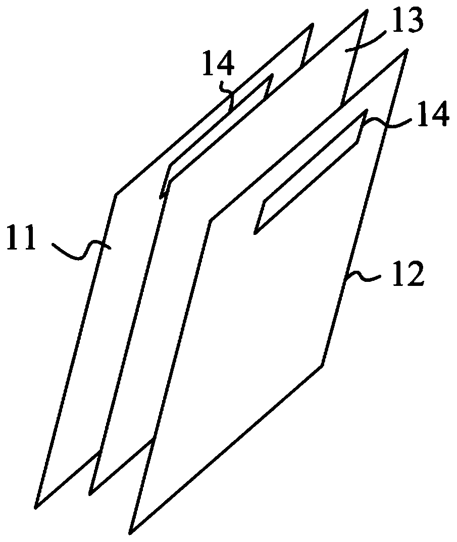
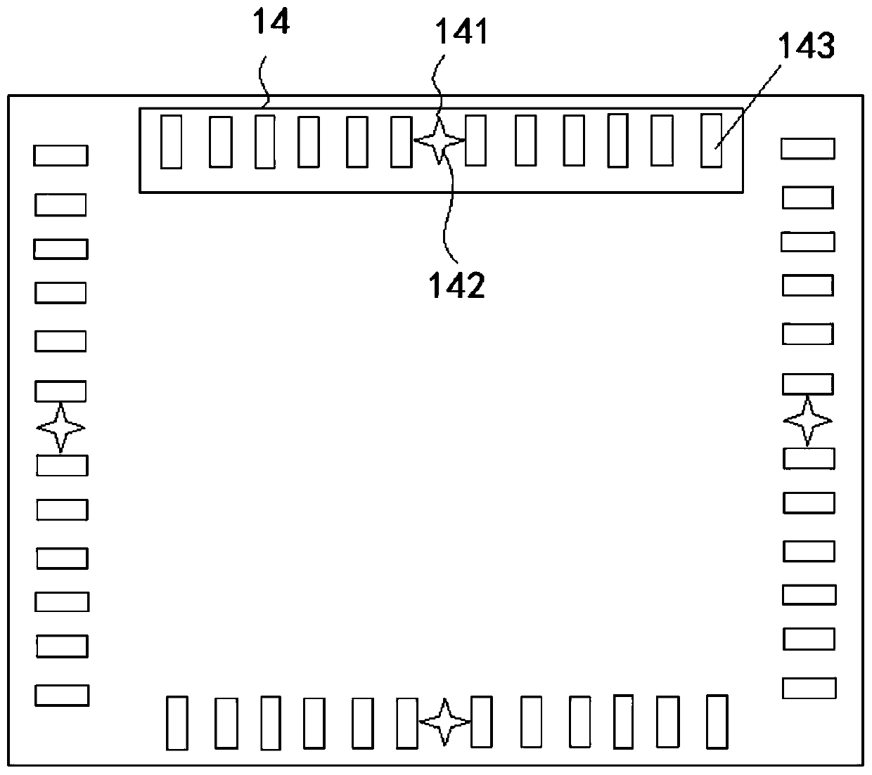
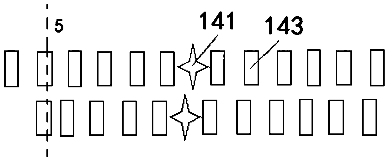
[0017] See Figure 1-2 As shown, the present invention relates to a double-sided PCB inspection module 100 based on a cursor.

[0018] The present invention discloses a double-sided PCB inspection module 100 based on a cursor. The double-sided PCB inspection module 100 has a first side 11 and a second side 12 and is clamped on the first side 11 and the second side. The dielectric material 13 between 12, the dielectric material 13 is a material that is translucent, translucent, or translucent after light. The first surface 11 and the second surface 12 are made of copper; the first surface 11 and the second surface 12 are provided with at least one cursor area 14 at opposite positions. The first position 141 is provided with a hollow hole 142, and with the hollow hole 142 as the center, offset marks 143 are arranged along a straight line to both sides of the first position 141, and the offset marks 143 are also hollow holes. The distance X between two adjacent offset marks 143 on...


PUM


Abstract

The invention discloses a vernier-based double-sided PCB detection module and an alignment method. The PCB detection module is provided with a first surface, a second surface and a dielectric materialclamped between the first surface and the second surface, and the first surface and the second surface are made of a copper material; at least one vernier area is arranged at the opposite positions of the first surface and the second surface. A hollow hole is formed in a first position in the vernier area; the first surface is provided with a hollow hole, offset marks are arranged on the two sides of the first position along a straight line with the hollow hole as the center, the offset marks are also hollow holes, the distance X between every two adjacent offset marks on the first face is equal, the distance Y between every two adjacent offset marks on the second face is equal, and the distance X is different from the distance Y. The layer deviation of the first surface and the second surface of the PCB detection module can be measured without using other external detection equipment, the measurement cost is low and the working efficiency is high.

Description

Technical field [0001] The invention relates to the field of PCB board measurement, in particular to a cursor-based double-sided PCB detection module and an alignment method. Background technique [0002] With the development of PCB boards to high-level and high-precision, the requirements for the accuracy of PCB board interlayer alignment are becoming more and more stringent, and the problem of PCB board layer deviation has attracted more and more attention. The PCB layer bias refers to the difference in concentricity between the layers of the PCB that originally required alignment. The scope of the requirements is controlled according to the design requirements of different PCB board types. The smaller the distance between the holes and the copper, the stricter the control is to ensure Its conduction and overcurrent capability. In the production process, the commonly used method to detect layer deviation is to add a set of concentric circles at the four corners of the PCB. Set...

Claims


Application Information

Patent Timeline
Patent Type & Authority Applications(China)
IPC IPC(8): G01N21/956G01N21/01
CPCG01N21/956G01N21/01G01N2021/95653
Inventor 叶国俊
Owner 鹤山市中富兴业电路有限公司
Why Eureka
Try Eureka