Thin film transistor and image display apparatus

一种薄膜晶体管、半导体的技术,应用在晶体管、半导体器件、电固体器件等方向,能够解决成本提高、成品率降低等问题,达到降低生产过程成本、高对比度、显示性能优越的效果

Active Publication Date: 2014-08-06
TOPPAN INC
View PDF5 Cites 6 Cited by
  • Summary
  • Abstract
  • Description
  • Claims
  • Application Information

AI Technical Summary

Problems solved by technology

Therefore, in order to obtain high precision, it is accompanied by difficulty, which also becomes the cause of cost increase and yield decrease

Method used


Image

  • Thin film transistor and image display apparatus
  • Thin film transistor and image display apparatus
  • Thin film transistor and image display apparatus

Examples


Embodiment 1

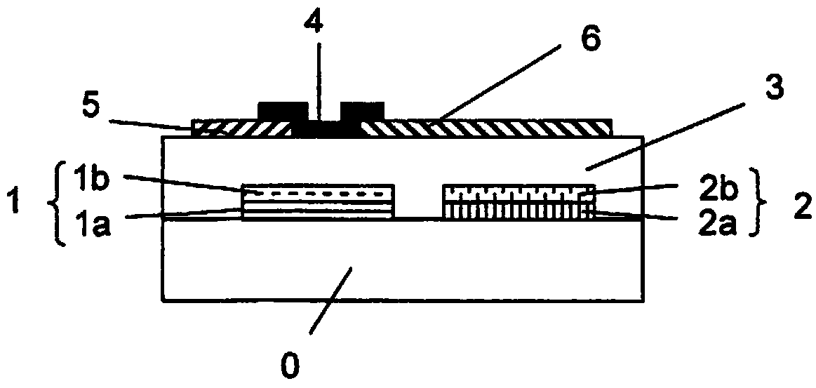
[0064] Next, Example 1 of the thin film transistor of this embodiment will be described based on the drawings.

[0065] figure 1 is a schematic diagram of the thin film transistor fabricated in Example 1.

[0066] In Example 1, produced as figure 1 The thin film transistor shown. Specifically, alkali-free glass 1737 produced by Corning Corporation was used as the insulating substrate 0, and the first layers 1a, 2a constituting the gate electrode 1 and the capacitor electrode 2 were formed on the insulating substrate 0 using a DC magnetron sputtering device. Room temperature deposition of ITO (thickness 100nm) and IGZO (thickness 10nm) constituting the second layers 1b, 2b. Next, gate electrode 1 and capacitor electrode 2 are formed from ITO and IGZO deposited at room temperature by simultaneous etching using photolithography. The input power for ITO film formation is 200W, the gas flow rate is Ar=100SCCM, O2=1SCCM, the film formation pressure is 1.0Pa, the input power for ...

Embodiment 2

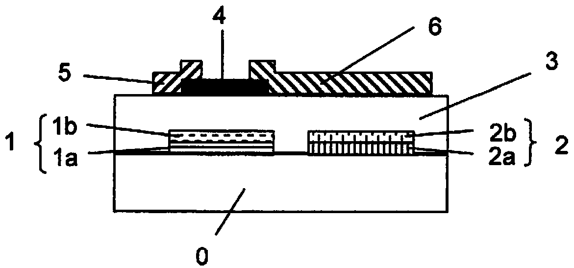
[0069] Next, Example 2 of the thin film transistor of this embodiment will be described based on the drawings.

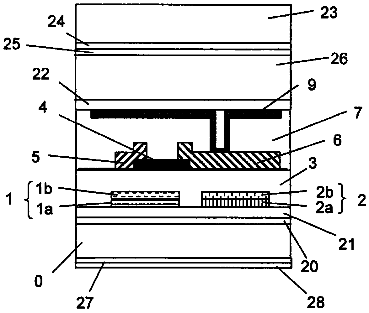
[0070] figure 2 It is a schematic cross-sectional view showing the structure of the thin film transistor of Example 2. image 3 It is a schematic cross-sectional view showing the structure of the image display device of the second embodiment.

[0071] In Example 2, produced as figure 2 TFTs as shown and as image 3 The image display device shown. Specifically, Corning's alkali-free glass 1737 was used as the insulating substrate 0 , and R (red) photosensitive resin was coated on the insulating substrate 0 by spin coating, and then patterned by photolithography. Similarly, the photosensitive resins G (green) and B (blue) were coated by spin coating, and then patterned by photolithography to form a color filter layer (color filter) 20 . Next, a light-transmitting resin is coated on the color filter layer 20 using a spin coating method to form the protective lay...


PUM

PropertyMeasurementUnit
currentaaaaaaaaaa
currentaaaaaaaaaa

Abstract

Since the gate electrode (1) and the capacitor electrode (2) are made into a double layer structure, the first layers (1a, 2a) in contact with the substrate (0) are made of ITO, and the second layers (1b, 2b) in contact with the gate insulating layer (3) are made of an metallic oxide layer, it becomes possible to form the gate electrode (1) and the capacitor electrode (2) having high optical transparency and high conductivity. Therefore, it becomes possible to improve the optical transparency of a thin film transistor and to improve the display performance of an image displaying apparatus for which the thin film transistor is used by using the above-described gate electrode (1) and the above-described capacitor electrode (2).

Description

technical field [0001] The present invention relates to a thin film transistor and an image display device that can be used for a driving element of an image display device and the like. Background technique [0002] Conventionally, thin film transistors using amorphous silicon, polycrystalline silicon, or the like have been used as transistors for driving electronic devices. However, amorphous silicon or polycrystalline silicon does not have light transmittance, and has light sensitivity in the visible light range, and thus requires a light shielding film. Therefore, when the thin film transistor exists on the front side of the display element of the display viewed from the viewing side of the display, it affects the visibility of the display. Therefore, the thin film transistor is arranged on the back side of the display element of the display. [0003] Color filters are generally used for colorization of reflective display devices such as reflective liquid crystal displ...

Claims


Application Information

Patent Timeline
Patent Type & Authority Applications(China)
IPC IPC(8): H01L29/786G02F1/1335G02F1/1368H01L21/28H01L21/336H01L29/423H01L29/49
CPCH01L27/127G02F2202/107H01L29/7869G02F1/1362H01L33/42H01L27/1255H01L27/1225G02F1/136286G02F1/136295H01L29/78606
Inventor 今村千寻伊藤学
Owner TOPPAN INC
Why Eureka
Try Eureka