

Semiconductor light emitting element and method for fabricating the same
A technology of light-emitting elements and manufacturing methods, which is applied to semiconductor devices, electrical components, circuits, etc., and can solve problems such as high manufacturing costs, inconvenience, and limited practicability
- Summary
- Abstract
- Description
- Claims
- Application Information
AI Technical Summary
Problems solved by technology
Method used
Image

Examples
Embodiment 1
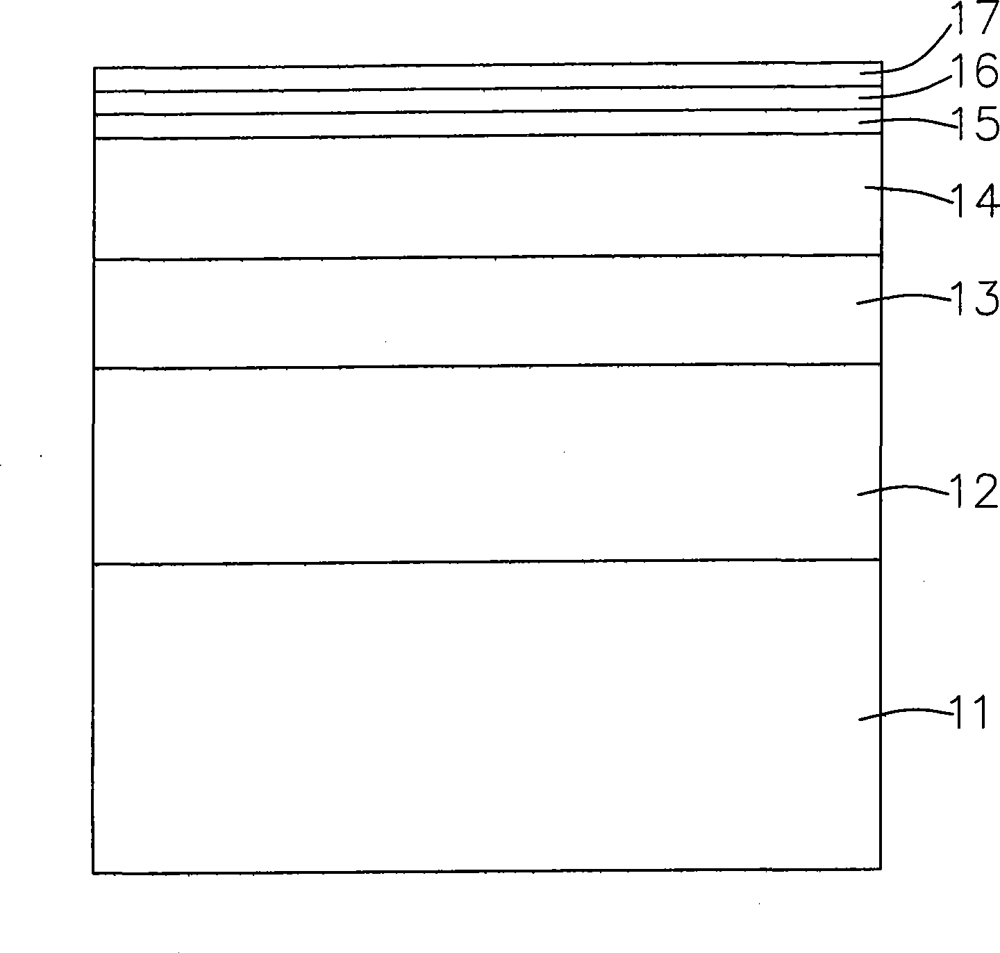
[0051] form semiconducting layered structure
[0052] see figure 1 Shown is a schematic diagram illustrating the structure and manufacturing process of Embodiment 1 of the semiconductor light-emitting element and its manufacturing method of the present invention. An n-type GaN n-type semiconductor layer 12, Light emitting layer 13 (multilayer quantum well structure of ten pairs of InGaN / GaN) and p-type semiconductor layer 14 of p-type GaN. Then use an electron beam evaporation system to deposit an indium tin oxide (ITO) transparent electrode material with a thickness of about 200 nm on the p-type semiconductor layer 14 as the current diffusion layer 15, and then deposit an aluminum metal layer with a thickness of about 500 nm on the current diffusion layer 15. As the reflective layer 16, it is used to improve the extraction of light.
[0053] Inverted semiconductor layered structure
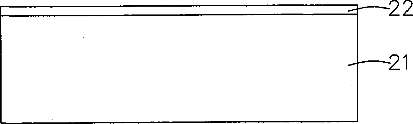
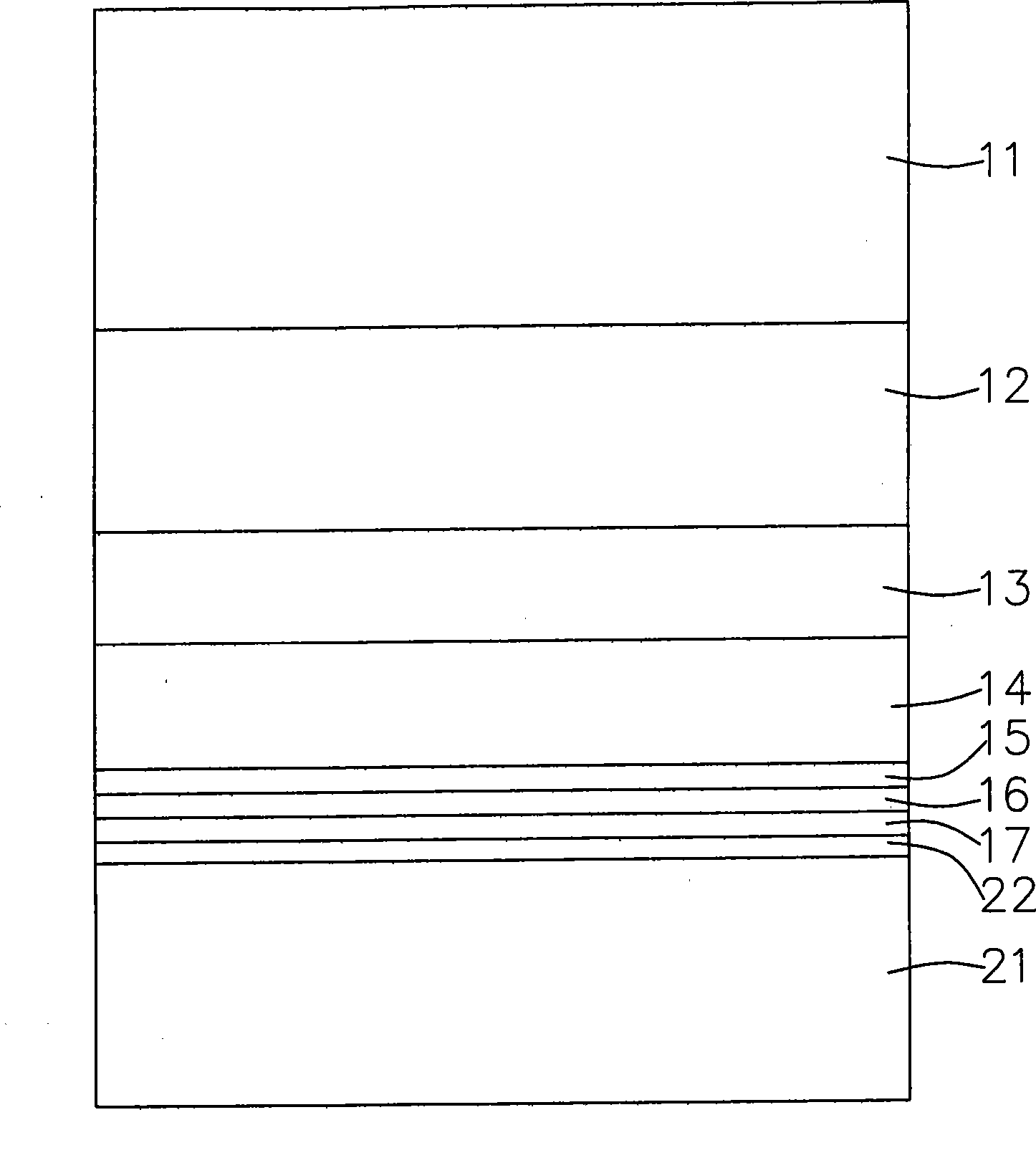
[0054] see Figure 1 ~ Figure 4 Shown is a schematic diagram illustrating the struc...
Embodiment 2
[0061]The implementation steps of Example 2 are roughly the same as those of Example 1, but the etching time is extended for five minutes in the etching process for forming nanopillars, so that the etching depth is about 1000nm, so as to form a nanocolumn with a length of about 1000nm in the direction perpendicular to the substrate. nanopillars.
PUM
| Property | Measurement | Unit |
|---|---|---|
| Section diameter | aaaaa | aaaaa |
| Thickness | aaaaa | aaaaa |
| Thickness | aaaaa | aaaaa |
Abstract
Description
Claims
Application Information