Pixel circuit, driving method thereof and display panel

A technology for pixel circuits and sub-circuits, applied in the field of pixel circuits and their driving methods and display panels, can solve problems such as insignificant effects, and achieve the effect of suppressing afterimages and suppressing the occurrence of

Active Publication Date: 2020-07-10
BOE TECH GRP CO LTD +1
View PDF5 Cites 1 Cited by
  • Summary
  • Abstract
  • Description
  • Claims
  • Application Information

AI Technical Summary

Problems solved by technology

Conventional methods try to improve the afterimage effect by changing the modulus and thickness of the gate insulating layer, the doping amount of the polysilicon layer, and the interface quality between the two layers, but the effect is not significant

Method used


Image

  • Pixel circuit, driving method thereof and display panel
  • Pixel circuit, driving method thereof and display panel
  • Pixel circuit, driving method thereof and display panel

Examples


Embodiment Construction

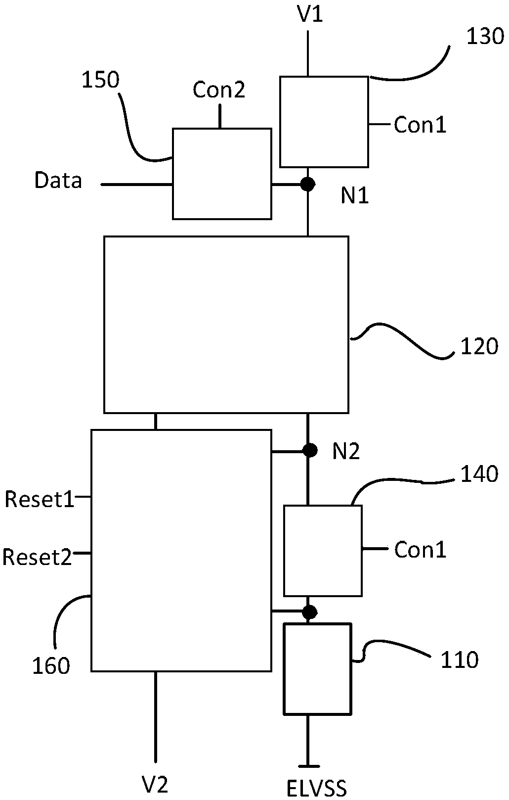
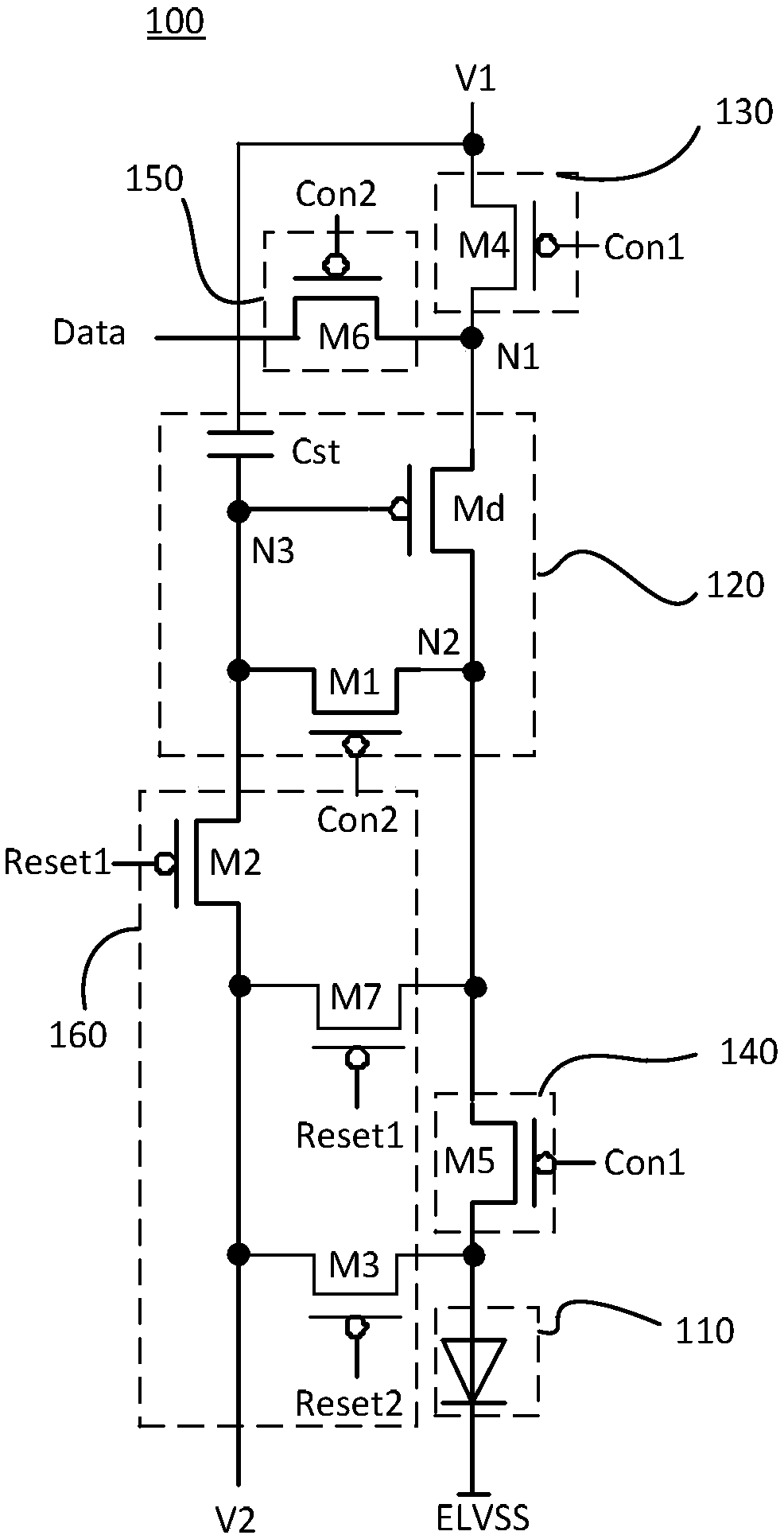
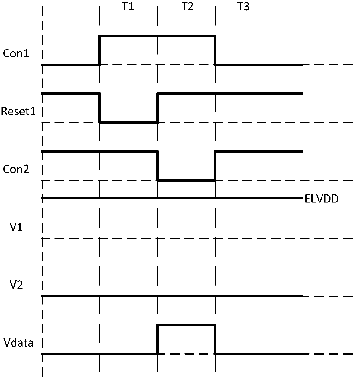
[0032] In order to make the purpose, technical solutions and advantages of the embodiments of the present disclosure clearer, the technical solutions in the embodiments of the present disclosure will be clearly and completely described below in conjunction with the drawings in the embodiments of the present disclosure. Apparently, the described embodiments are some, not all, of the embodiments of the present disclosure. Based on the described embodiments of the present disclosure, all other embodiments obtained by persons of ordinary skill in the art without creative effort fall within the protection scope of the present disclosure. It should be noted that throughout the drawings, the same elements are denoted by the same or similar reference numerals. In the following description, some specific embodiments are only for the purpose of description, and should not be construed as limiting the present disclosure in any way, but are only examples of the embodiments of the present ...


PUM


Abstract

The invention provides a pixel circuit, a driving method thereof and a display panel. The pixel circuit includes: a light emitting element; a driving sub-circuit configured to generate a current for causing the light emitting element to emit light; a first light-emitting control sub-circuit and the second light-emitting control sub-circuit, respectively configured to supply current for enabling the light-emitting element to emit light to the first end of the light-emitting element under the control of a first control signal; a driving control sub-circuit, configured to provide the data voltagesignal to the driving sub-circuit under the control of the second control signal; and a reset sub-circuit, configured to use the second voltage to reset the driving sub-circuit, the first end of thelight-emitting element and the second node under the control of the first reset signal and the second reset signal.

Description

technical field [0001] The present disclosure relates to the field of display technology, and in particular to a pixel circuit, a driving method thereof, and a display panel. Background technique [0002] In an OLED (Organic Light Emitting Diode, Organic Light Emitting Diode) display device, due to the hysteresis effect of the driving transistor, afterimages may occur. Conventional methods attempt to improve the afterimage effect by changing the modulus and thickness of the gate insulating layer, the doping amount of the polysilicon layer, and the interface quality between the two layers, but the effect is not significant. Contents of the invention [0003] The disclosure proposes a pixel circuit, a driving method thereof, and a display panel. [0004] According to one aspect of the present disclosure, a pixel circuit is provided. The pixel circuit includes: a light emitting element; a driving subcircuit configured to generate current for making the light emitting elemen...

Claims


Application Information

Patent Timeline
Patent Type & Authority Applications(China)
IPC IPC(8): G09G3/3225
CPCG09G3/3225G09G2320/0257G09G2300/0426G09G2300/0842G09G2300/0814G09G2300/0819G09G3/3233
Inventor 黄应龙杨炳伟高文宝
Owner BOE TECH GRP CO LTD
Why Eureka
Try Eureka