Anti-coupling-interference power supply generation circuit

A technology for coupling interference and generating circuits, which is applied in the field of power generating circuits and can solve problems such as exceeding the breakdown voltage

Pending Publication Date: 2020-07-10
SHANGHAI HUAHONG GRACE SEMICON MFG CORP
View PDF2 Cites 1 Cited by
  • Summary
  • Abstract
  • Description
  • Claims
  • Application Information

AI Technical Summary

Problems solved by technology

[0004] However, when the power supply circuit in the related art is working in the discharge stage, since the output node VP of the discharge path is coupled and conducted with the output node VDI of the power generation circuit, the output node VP discharges to the potential of the output node VDI, so that the output node VP will output The potential of the node VDI is pulled up. If the potential of the output node VDI is pulled up to exceed the threshold, there will be a risk of exceeding the breakdown voltage

Method used


Image

  • Anti-coupling-interference power supply generation circuit
  • Anti-coupling-interference power supply generation circuit
  • Anti-coupling-interference power supply generation circuit

Examples


Embodiment 1

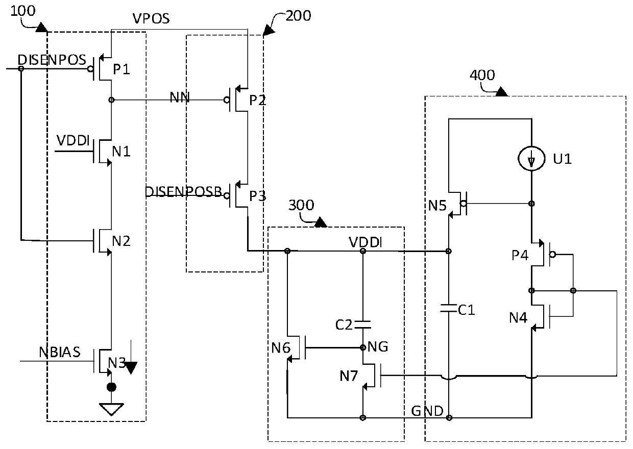
[0035] This embodiment provides an anti-coupling interference power generating circuit, refer to figure 2 , the anti-coupling interference power generation circuit includes:

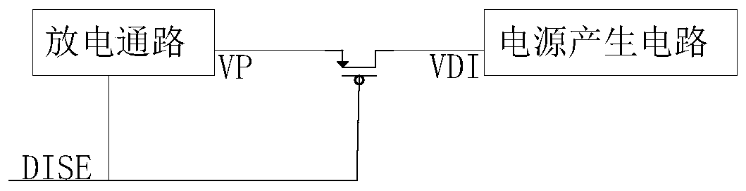
[0036] The first discharge path 100, the high-voltage input node VPOS of the first discharge path 100 is connected to the first voltage, the first voltage is a high voltage, and the control terminal of the first discharge path 100 is connected to the first control signal DISENPOS for the first In the discharge stage, the high-voltage input node VPOS is discharged;

[0037] The second discharge path 200, the second discharge path 200 is connected between the first discharge path 100 and the power generation path 400, the control terminal of the first discharge path 100 is connected to the second control signal DISENPOSB, the transfer node NN of the second discharge path 200 connected to the first discharge path 100; used to discharge the high voltage input node VPOS to the potential of the power output ...

Embodiment 2

[0043] This embodiment is on the basis of embodiment 1, with reference to figure 2 An anti-coupling interference power generation circuit is provided, and the anti-coupling interference power generation circuit includes:

[0044] The first discharge path 100, the first discharge path 100 includes the first PMOS transistor P1, the first NMOS transistor N1, the second NMOS transistor N2 and the third NMOS transistor N3 connected in series; the gate of the first PMOS transistor P1 is the first discharge The control terminal of the channel 100, the source of the first PMOS transistor P1 is connected to the first voltage, the drain of the first PMOS transistor P1 is connected to the drain of the first NMOS transistor N1; the gate of the first NMOS transistor N1 is connected to the power supply output node VDDI , the source of the first NMOS transistor N1 is connected to the drain of the second NMOS transistor N2; the gate of the second NMOS transistor N2 is connected to the gate o...

Embodiment 3

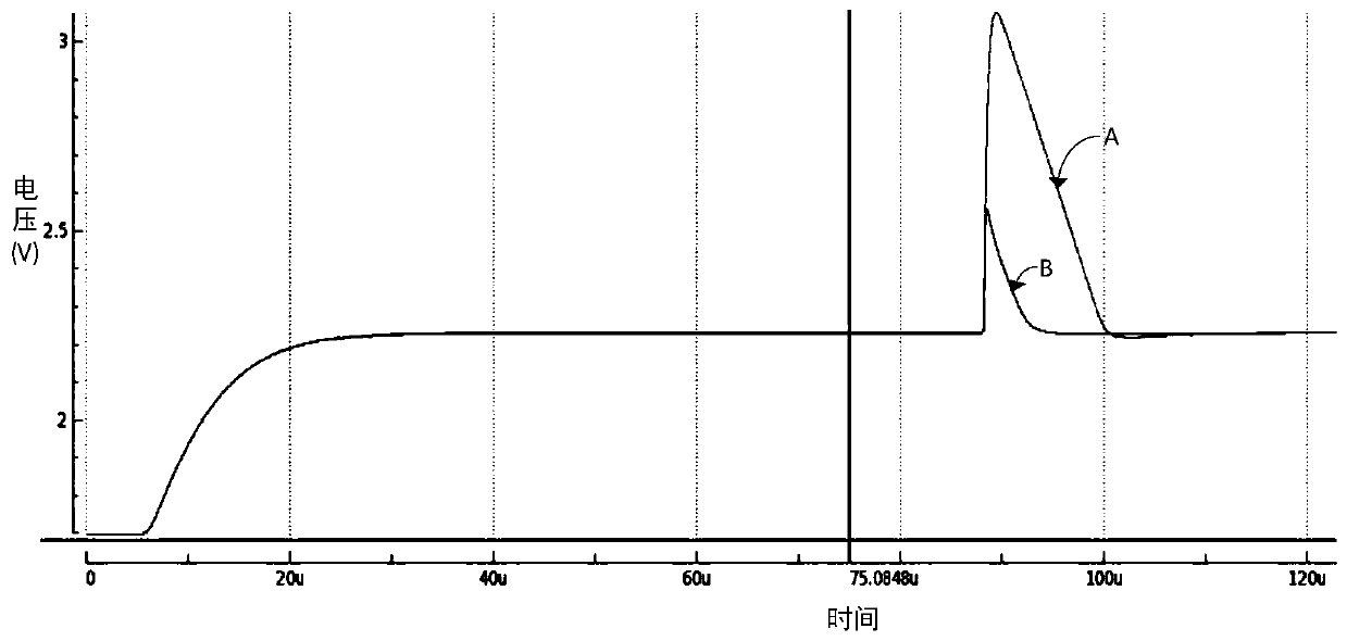
[0054] In this embodiment, on the basis of implementation 2, in order to prevent the potential of the anti-coupling interference control node NG from turning on the sixth NMOS transistor N6 in the initial state, the anti-coupling interference control node NG is quickly pulled down when the potential of the anti-coupling interference control node NG is raised. The potential of the coupling interference control node NG, the anti-coupling interference circuit 300 also includes a seventh NMOS transistor N7, the gate of the seventh NMOS transistor N7 is connected to the power generation channel 400, the source of the seventh NMOS transistor N7 is grounded, and the seventh NMOS transistor N7 The drain of N7 is connected to the anti-coupling interference control node NG.

[0055] Specifically, the gate of the seventh NMOS transistor N7 is connected to the gates of the fourth PMOS transistor P4 and the fourth NMOS transistor N4, and the seventh NMOS transistor N7 can be mirrored to gen...


PUM


Abstract

The invention relates to a semiconductor integrated circuit, in particular to an anti-coupling-interference power supply generation circuit, which comprises a first discharge path, wherein a high-voltage input node of the first discharge path is connected with a first voltage, and a control end of the first discharge path is connected with a first control signal, and the first discharge path is used for discharging a high-voltage input node in a first discharge stage; a second discharge path which is connected between the first discharge path and a power supply generation path, wherein the control end of the first discharge path is connected with a second control signal, and the transmission node of the second discharge path is connected with the first discharge path, and the second discharge path is used for discharging the high-voltage input node to the potential of the power supply output node on the power supply generation path in a second discharge stage; and an anti-coupling-interference circuit which is connected between the second discharge path and the power supply generation path and is used for lowering the potential of the power supply output node in the second discharge stage. The anti-coupling-interference circuit can reduce the potential of the power supply output node in the second discharge stage, thereby avoiding breakdown voltage.

Description

technical field [0001] The present application relates to a semiconductor integrated circuit, in particular to a power generating circuit anti-coupling and interference. Background technique [0002] In order to reduce the power consumption in the semiconductor device and reduce the external voltage supplied to the semiconductor device, a discharge path is usually provided in the power supply circuit. [0003] The power supply circuit in the related art refers to figure 1 , including a discharge path and a power generation circuit, the output node VP of the discharge path is connected to the output node VDI of the power generation circuit in the discharge phase, and the control signal DISE can control the discharge path to work in the discharge phase. [0004] However, when the power supply circuit in the related art is working in the discharge stage, since the output node VP of the discharge path is coupled and conducted with the output node VDI of the power generation cir...

Claims


Application Information

Patent Timeline
Patent Type & Authority Applications(China)
IPC IPC(8): H02M1/44H02M1/32
CPCH02M1/44H02M1/32H02M1/0038
Inventor 马媛邵博闻
Owner SHANGHAI HUAHONG GRACE SEMICON MFG CORP
Why Eureka
Try Eureka