Semiconductor structure and forming method thereof

A semiconductor and fin technology, applied in the field of semiconductor structure and its formation, can solve the problems of difficult channel and poor channel control ability of gate structure, so as to reduce the probability of bending, improve performance and performance uniformity , the effect of high rigidity

Active Publication Date: 2020-07-14
SEMICON MFG INT (SHANGHAI) CORP +1
View PDF10 Cites 0 Cited by
  • Summary
  • Abstract
  • Description
  • Claims
  • Application Information

AI Technical Summary

Problems solved by technology

However, as the channel length of the device is shortened, the distance between the source and the drain of the device is also shortened, so the ability of the gate structure to control the channel becomes worse, and the gate voltage pinches off the channel. The difficulty of the channel is also increasing, making the phenomenon of subthreshold leakage (subthreshold leakage), the so-called short-channel effect (short-channel effects, SCE) more prone to occur

Method used


Image

  • Semiconductor structure and forming method thereof
  • Semiconductor structure and forming method thereof
  • Semiconductor structure and forming method thereof

Examples


Embodiment Construction

[0012] It can be seen from the background art that the devices formed so far still have the problem of poor performance. The reasons for the poor performance of the device are analyzed in conjunction with a method of forming a semiconductor structure.

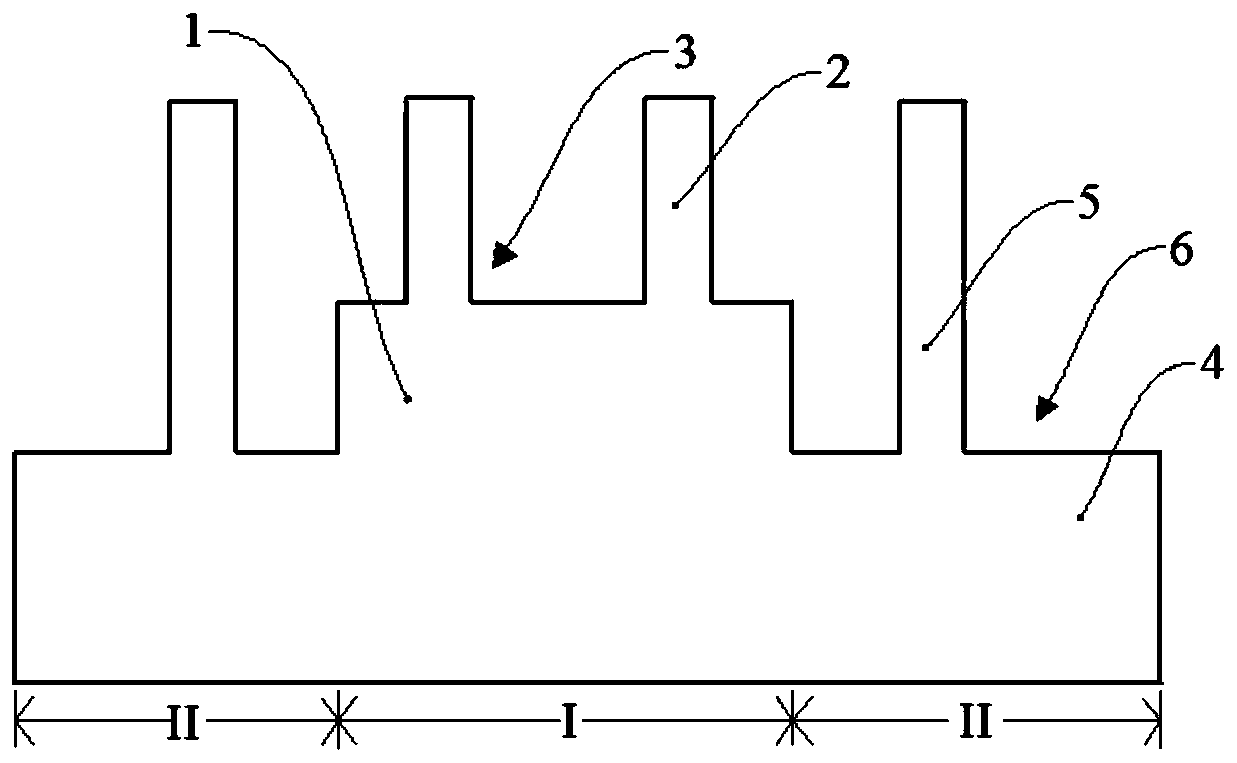
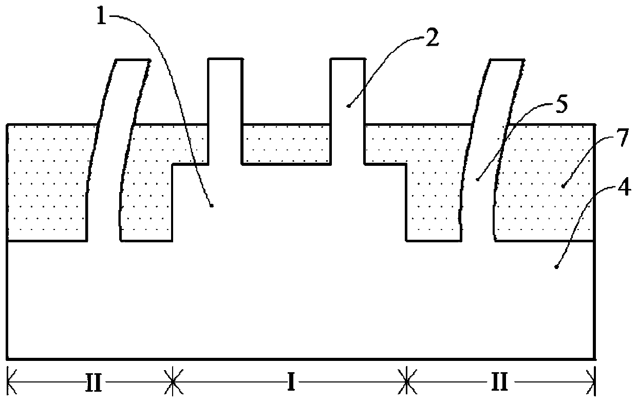
[0013] refer to Figure 1 to Figure 2 , shows a structural schematic diagram corresponding to each step in a method for forming a semiconductor structure.

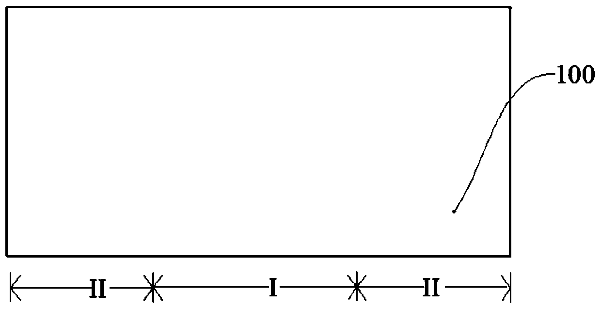
[0014] refer to figure 1 , forming a substrate 4 and fins protruding from the substrate 4, the substrate 4 includes a first region I and a second region II, the first region I is used to form a first device, the second region The second region II is used to form the second device, the power of the second device is lower than the power of the first device; the region between the fins of the first region is the first groove, and the fins of the second region are The area between the parts is the second groove, and the depth of the second groove 6 is greater than the depth ...


PUM

PropertyMeasurementUnit
Thicknessaaaaaaaaaa

Abstract

The invention discloses a semiconductor structure and a forming method thereof, and the forming method comprises the steps: etching a substrate of a first region, and forming first fin parts and firstgrooves located between the first fin parts; etching the substrate in the second region to form second fin parts and second grooves located between the second fin parts, wherein the second fin partscomprises bottom fin parts and top fin parts located on the bottom fin parts, and the width of the bottom fin parts is greater than the width of the first fin parts in the direction perpendicular to the extension direction of the second fin part, and the depth of the second groove is greater than that of the first groove; and forming a first isolation layer in the second groove, wherein the firstisolation layer at least covers the bottom fin part. According to the embodiment of the invention, the rigidity of the second fin part is higher by increasing the width of the bottom fin part, and thecapability of the second fin part for bearing the stress of the first isolation layer is correspondingly higher, so the probability that the second fin part is bent due to the stress of the first isolation layer is reduced, and the performance and the performance uniformity of the device are improved.

Description

technical field [0001] Embodiments of the present invention relate to the field of semiconductor manufacturing, and in particular, to a semiconductor structure and a method for forming the same. Background technique [0002] In semiconductor manufacturing, with the development trend of ultra-large-scale integrated circuits, the feature size of integrated circuits continues to decrease. In order to adapt to smaller feature sizes, metal-oxide-semiconductor field-effect transistors (Metal-Oxide-Semiconductor Field-Effect Transistor , MOSFET) channel length has been shortened accordingly. However, as the channel length of the device is shortened, the distance between the source and the drain of the device is also shortened, so the ability of the gate structure to control the channel becomes worse, and the gate voltage pinches off the channel. The channel becomes more and more difficult, making subthreshold leakage (subthreshold leakage), the so-called short-channel effect (shor...

Claims


Application Information

Patent Timeline
IPC IPC(8): H01L21/8234H01L27/088
CPCH01L21/823431H01L21/823412H01L27/0886
Inventor 周飞
Owner SEMICON MFG INT (SHANGHAI) CORP
Why Eureka
Try Eureka