A display panel and electronic device

A technology for display panels and electronic devices, used in circuits, electrical components, photovoltaic power generation, etc., can solve the problems of color difference and low life, and achieve the effect of ensuring light transmittance

Active Publication Date: 2022-06-07
WUHAN CHINA STAR OPTOELECTRONICS SEMICON DISPLAY TECH CO LTD
View PDF0 Cites 0 Cited by
  • Summary
  • Abstract
  • Description
  • Claims
  • Application Information

AI Technical Summary

Problems solved by technology

In the case that the arrangement of the original pixels remains unchanged, no matter the number of intermediate pixels is removed in equal proportions (such as figure 1 As shown in part a), or remove pixels by the smallest repeating unit (such as figure 1 (as shown in part b), during the display process of the display panel, the luminous brightness of the pixels in the CUP area is required to be greater than the luminous brightness of the pixels in the other display areas (Active Area, hereinafter referred to as AA area), so that the lifetime of the pixels in the CUP area is lower than that of other display areas. AA area
In this way, after the display panel is used for a long time, there will be a color difference between the CUP area and other AA areas.

Method used


Image

  • A display panel and electronic device
  • A display panel and electronic device
  • A display panel and electronic device

Examples


Embodiment Construction

[0021] Embodiments of the present invention are described in detail below, examples of which are illustrated in the accompanying drawings, wherein the same or similar reference numerals refer to the same or similar components or components having the same or similar functions throughout. The embodiments described below with reference to the accompanying drawings are exemplary, only used to explain the present invention, and should not be construed as a limitation of the present invention. Furthermore, the present disclosure repeats reference numerals and / or reference letters in various instances for the purpose of simplicity and clarity and does not in itself indicate a relationship between the various embodiments and / or arrangements discussed.

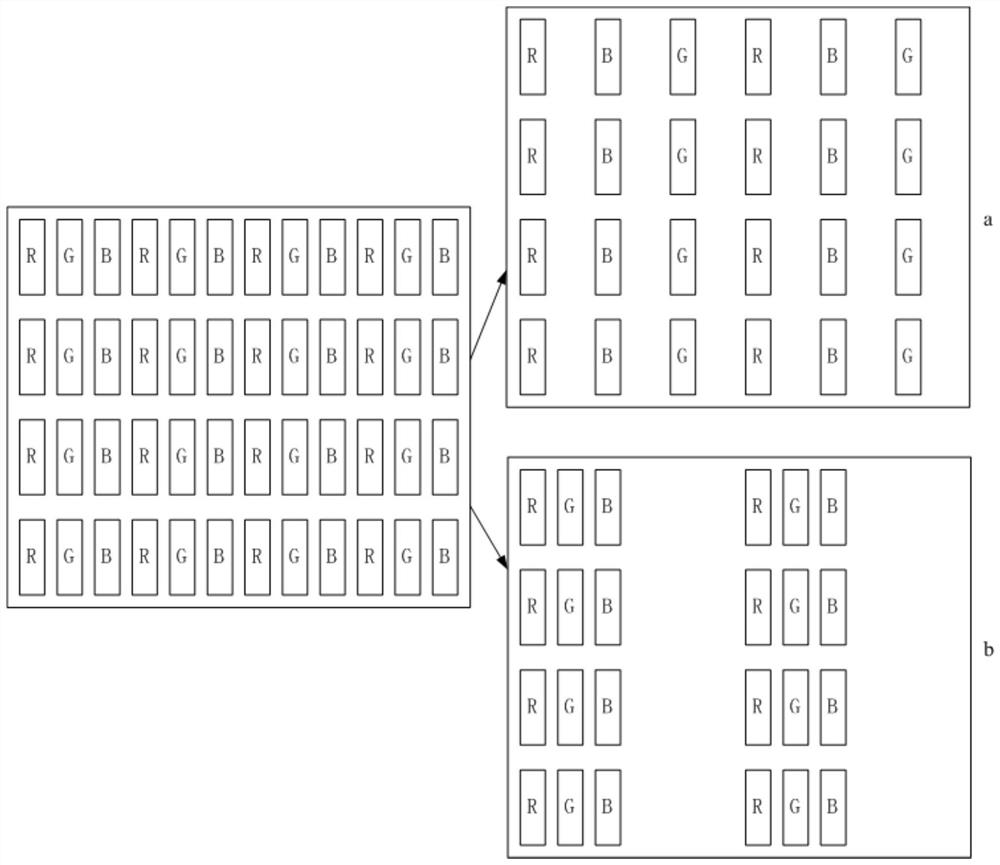
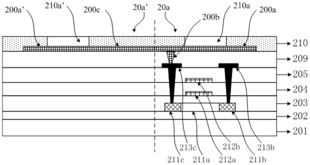
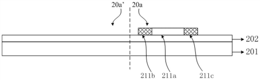
[0022] The display panel of the present invention has an optical sensor area, the optical sensor area corresponds to the optical sensor, and the display panel includes a plurality of light-emitting units located in the optical sensor a...


PUM


Abstract

The invention discloses a display panel and an electronic device. The display panel has an optical sensor area corresponding to the optical sensor. The display panel includes a plurality of light emitting units located in the optical sensor area; the light emitting unit includes a first light emitting subunit and at least one The second light emitting subunit, the first light emitting subunit includes a pixel driving circuit. The present invention drives at least two light-emitting sub-units to emit light through a pixel driving circuit, which can reduce the routing density of the array substrate in the optical sensor area, and does not need to increase the brightness of the pixels in the optical sensor area during the display of the display panel, thereby ensuring the high brightness of the display panel. Light transmission in the optical sensor area without reducing the lifetime of the pixels therein.

Description

technical field [0001] The present invention relates to the field of display technology, and in particular, to a display panel and an electronic device. Background technique [0002] In recent years, the rapid development of OLED (Organic Light Emitting Diode, organic light-emitting diode) display technology has promoted the rapid entry of curved and flexible display products into the market, and technological updates in related fields are also changing with each passing day. OLED refers to a diode that uses organic semiconductor materials and light-emitting materials to emit light through carrier injection and recombination driven by an electric field. Due to the advantages of light weight, self-illumination, wide viewing angle, low driving voltage, high luminous efficiency, low power consumption, and fast response speed, OLED display devices are widely used. [0003] AMOLED (Active-Matrix Organic Light Emitting Diode, Active-Matrix Organic Light Emitting Diode) display de...

Claims


Application Information

Patent Timeline
Patent Type & Authority Patents(China)
IPC IPC(8): H01L27/32
CPCH10K59/00H10K59/35H10K59/12H10K59/1213H10K59/13Y02E10/549
Inventor 向明彭宁昆胡俊艳
Owner WUHAN CHINA STAR OPTOELECTRONICS SEMICON DISPLAY TECH CO LTD
Why Eureka
Try Eureka