Integrated Fan-Out Device, three dimensional integrated circuit System, and manufacturing Method thereof

A fan-out, integrated passive technology, applied in the direction of circuits, electrical components, electrical solid devices, etc., can solve the problem of complex utilization of bonding technology

Inactive Publication Date: 2020-08-07
TAIWAN SEMICON MFG CO LTD
View PDF0 Cites 2 Cited by
  • Summary
  • Abstract
  • Description
  • Claims
  • Application Information

AI Technical Summary

Problems solved by technology

This bonding process utilizes complex technology, so it would be desirable to improve it

Method used


Image

  • Integrated Fan-Out Device, three dimensional integrated circuit System, and manufacturing Method thereof
  • Integrated Fan-Out Device, three dimensional integrated circuit System, and manufacturing Method thereof
  • Integrated Fan-Out Device, three dimensional integrated circuit System, and manufacturing Method thereof

Examples


Embodiment Construction

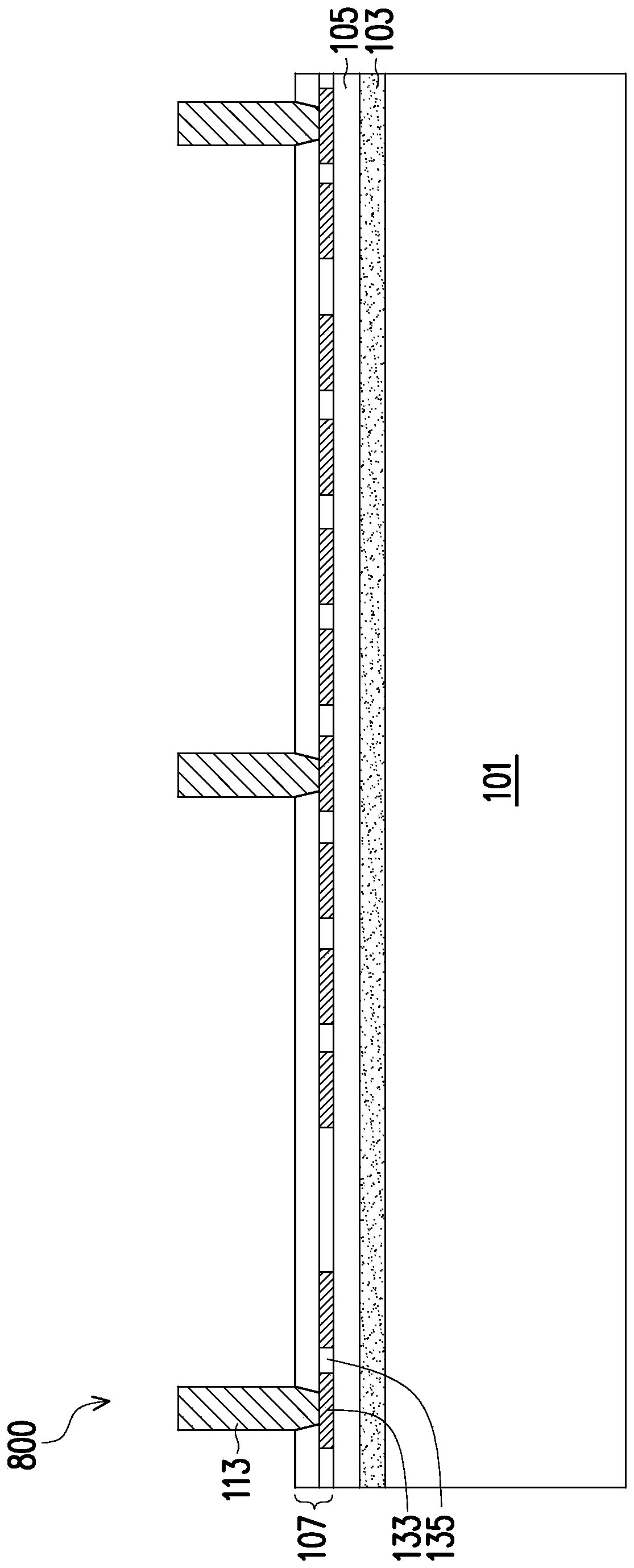
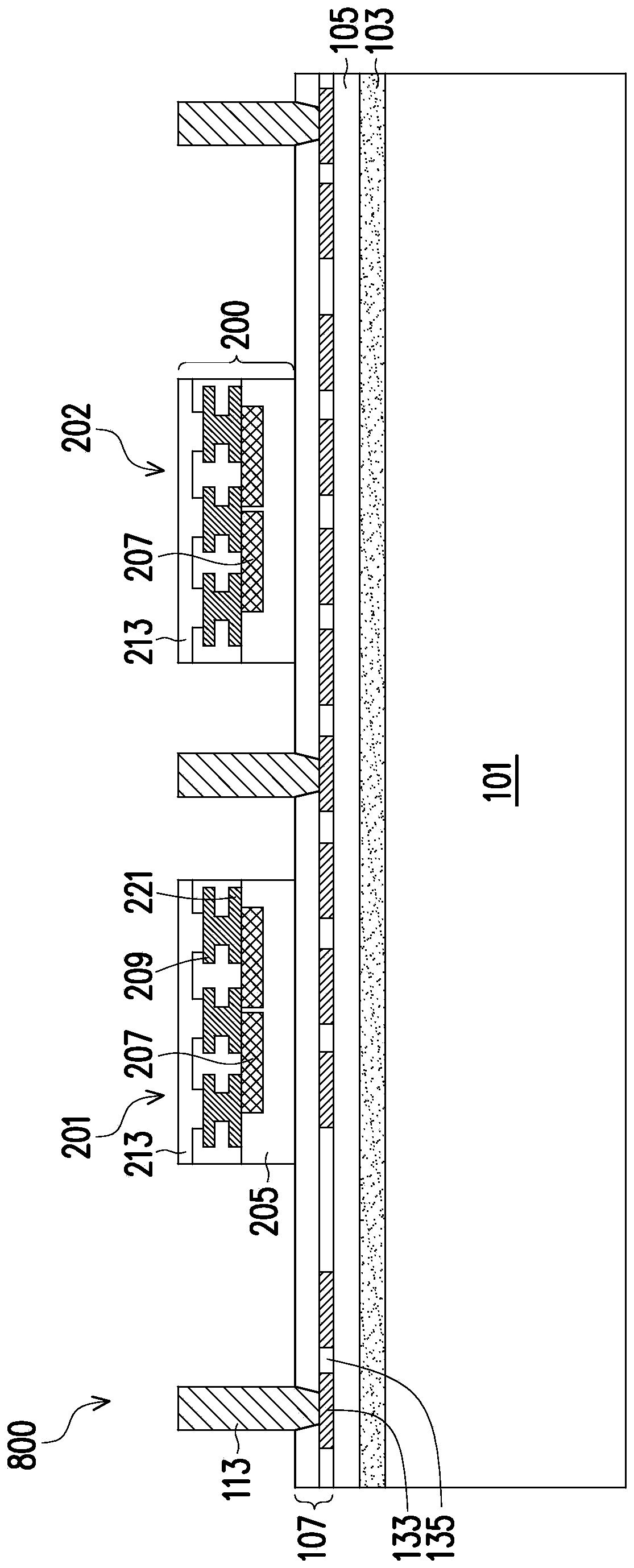
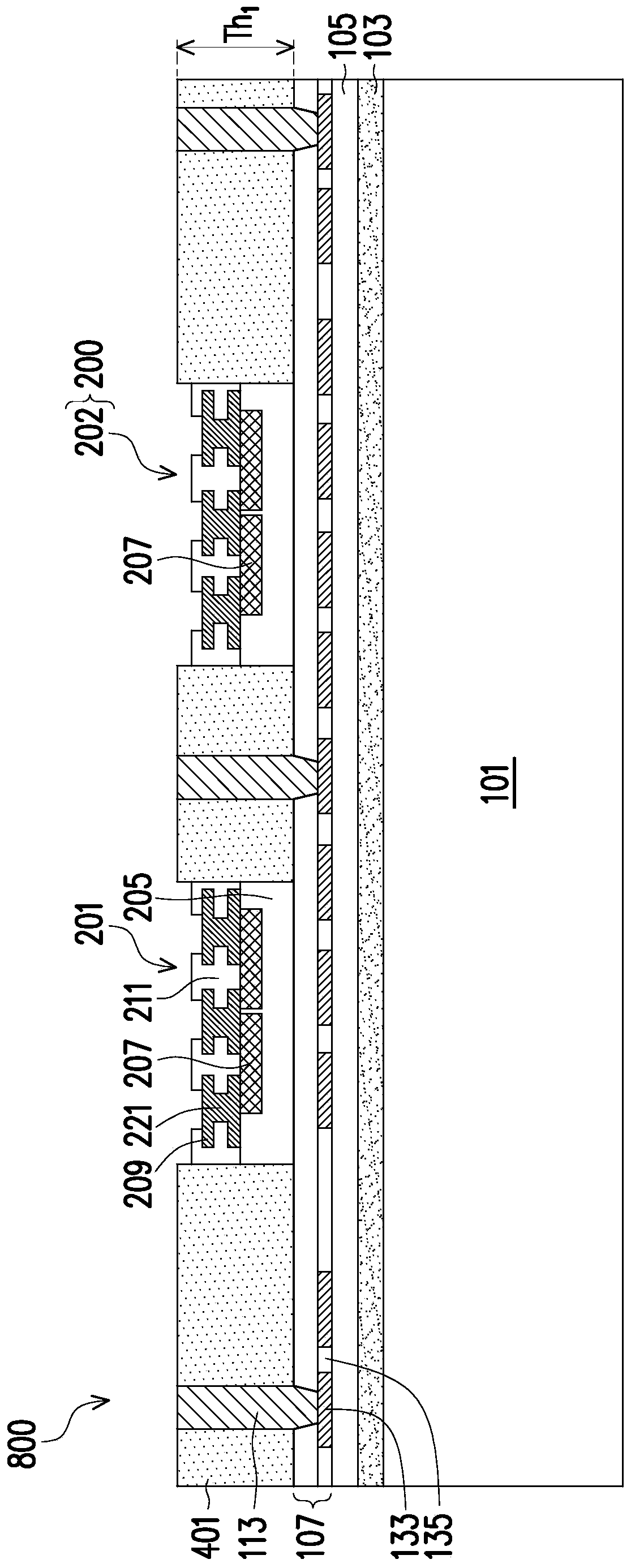
[0113] The following disclosure provides many different embodiments, or examples, for implementing different features of embodiments of the invention. Specific examples of components and arrangements are set forth below to simplify the present disclosure. Of course, these are examples only and are not intended to be limiting. For example, the description below that a first feature is formed "on" a second feature or "on" a second feature may include embodiments in which the first and second features are formed in direct contact, and may also include An embodiment wherein an additional feature may be formed between the first feature and the second feature such that the first feature may not be in direct contact with the second feature. Additionally, this disclosure may reuse reference numbers and / or letters in various instances. Such re-use is for brevity and clarity and does not in itself indicate a relationship between the various embodiments and / or configurations discussed....


PUM


Abstract

Embodiments of the invention are about an integrated Fan-Out Device, a three dimensional integrated circuit System, and a manufacturing Method thereof. A three dimensional integrated circuit (3D-IC) module socket system includes an integrated Fan-Out (InFO) adapter having one or more integrated passive devices (IPDs) embedded in the InFO adapter. The InFO adapter is also integrated into the 3D-ICmodule socket system by stacking the InFO adapter between a socket and a SoW package. The InFO adapter with embedded IPDs allows for more planar area of the SoW package to be available for interfacingthe socket and provides a short distance between the embedded IPDs and computing dies of the SoW package which enhances a power distribution network (PDN) performance and improves current handling ofthe 3D-IC module socket system.

Description

technical field [0001] Embodiments of the present invention relate to an integrated fan-out device, a three-dimensional integrated circuit system and a manufacturing method thereof. Background technique [0002] The semiconductor industry has experienced rapid growth due to the continued increase in the integration density of various electronic components (eg, transistors, diodes, resistors, capacitors, etc.). In large part, this increase in integration density is due to successive reductions in minimum feature size (for example, shrinking semiconductor process nodes toward the sub-20nm node), which has enabled more Many components can be integrated in a given area. With the recent increase in demand for miniaturization, higher speed, greater bandwidth, lower power loss, and less delay, the need for smaller and more innovative semiconductor die packaging technologies has also increased. increasing. [0003] As semiconductor technology develops further, stacked and bonded ...

Claims


Application Information

Patent Timeline
Patent Type & Authority Applications(China)
IPC IPC(8): H01L23/64H01L23/488
CPCH01L23/64H01L24/02H01L2224/02331H01L2224/02379H01L23/49816H01L23/5383H01L23/49833H01L23/49822H01L21/6835H01L2221/68345H01L2221/68359H01L2221/68372H01L2221/68331H01L21/568H01L21/561H01L2221/68313H01L21/56H01L23/3128H01L2224/04105H01L2224/12105H01L2224/73267H01L2224/92244H01L2224/97H01L2224/32225H01L2924/18162H01L24/19H01L2924/3512H01L2225/1035H01L2225/1058H01L2224/16227H01L2224/73205H01L2224/92125H01L2224/81005H01L2924/19105H01L2924/19011H01L24/16H01L24/32H01L24/73H01L24/92H01L24/20H01L24/97H01L25/105H01L25/50H01L2224/83H01L23/32H01L24/33H01L24/09H01L23/481H01L21/565H01L27/0688H01L2224/02372H01L23/3178
Inventor 赖昱嘉谢政杰余振华刘重希蔡豪益郭庭豪
Owner TAIWAN SEMICON MFG CO LTD
Why Eureka
Try Eureka