Display panel, manufacturing method thereof and display device

A technology for display panels and graphics, applied in the field of display panels and display devices, capable of solving problems such as abnormal brightness of display panels and affecting display quality of display panels

Pending Publication Date: 2020-08-07
BOE TECH GRP CO LTD
View PDF4 Cites 10 Cited by
  • Summary
  • Abstract
  • Description
  • Claims
  • Application Information

AI Technical Summary

Problems solved by technology

[0004] The object of the present invention is to provide a display panel, its manufacturing method, and a display device, which are used to solve the problem that when the display panel is in the light-emitting state, the voltage jump of the d

Method used


Image

  • Display panel, manufacturing method thereof and display device
  • Display panel, manufacturing method thereof and display device
  • Display panel, manufacturing method thereof and display device

Examples


Embodiment Construction

[0070] In order to further illustrate the display panel, the manufacturing method thereof, and the display device provided by the embodiments of the present invention, a detailed description will be given below in conjunction with the accompanying drawings.

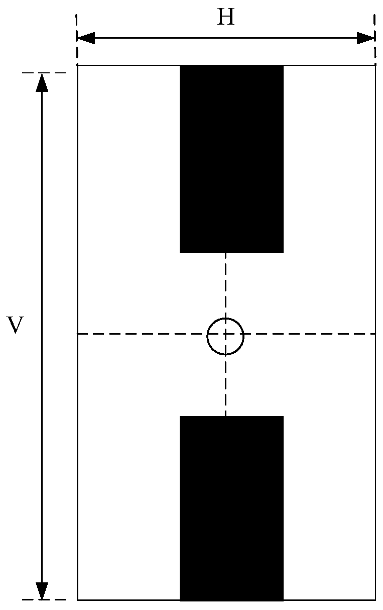
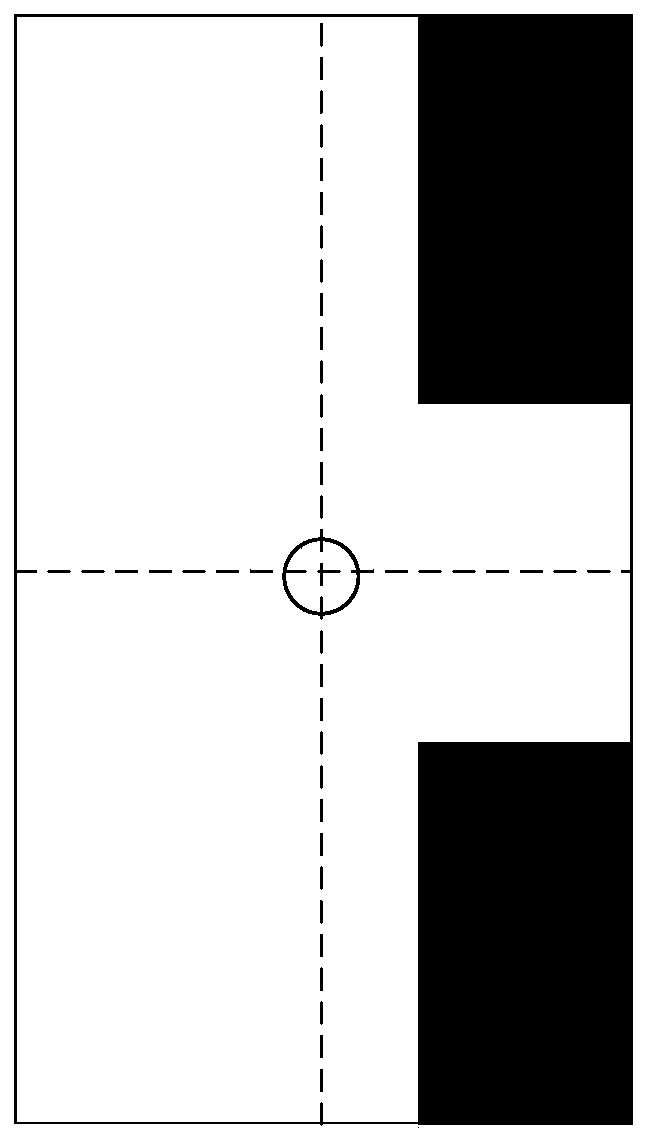
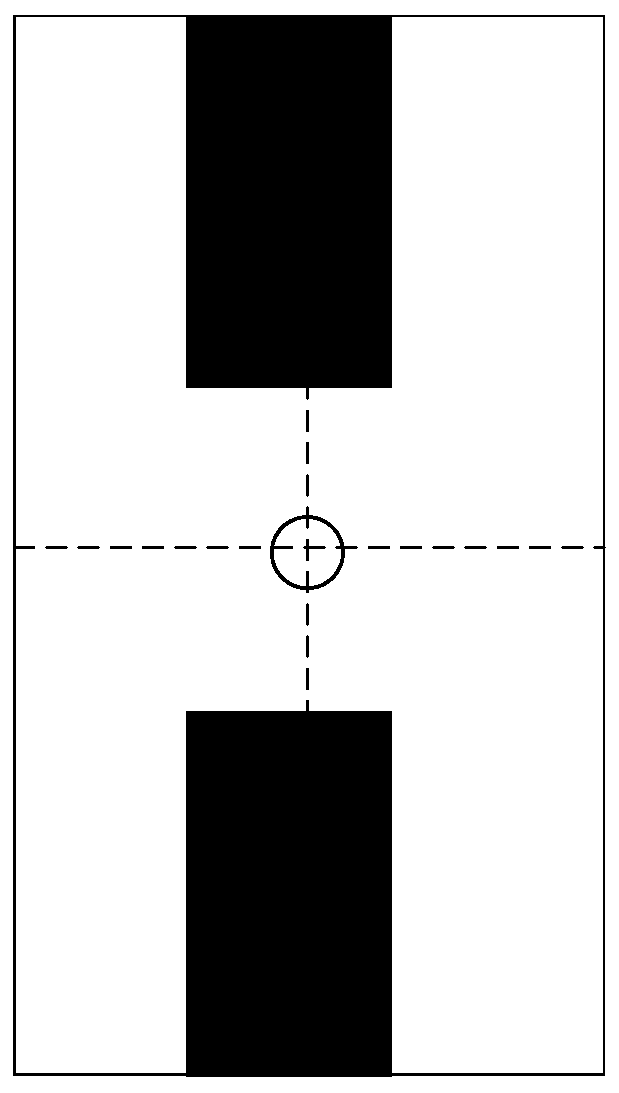
[0071] Crosstalk is an important evaluation index of the display panel. Crosstalk is divided into horizontal crosstalk (H-talk) and vertical crosstalk (V-talk). For the pixel circuit of 9T1C (nine transistors and one storage capacitor) , V-talk is relatively serious. After analysis, when the sub-pixel drive circuit drives the light-emitting unit to be in the light-emitting state after compensation, the data voltage jump of the transmission band on the data line pattern will drive the gate of the drive transistor in the sub-pixel drive circuit to change through the parasitic capacitance, and then As a result, the display brightness of some areas of the display panel is abnormal.

[0072] Such as 1a~ Figure 1d As shown, ...


PUM


Abstract

The invention provides a display panel, a manufacturing method of the display panel and a display device, relates to the technical field of the display. The invention aims to solve the problem that the voltage jump of a data signal in the display panel drives the grid voltage of a driving transistor to change through a parasitic capacitor, so that the brightness of a part of area of the display panel is abnormal. In a sub-pixel driving circuit of the display panel, a grid electrode of a driving transistor is coupled with a second electrode of a second transistor through a fourth conductive connecting part, and a second polar plate of a storage capacitor is coupled with a second electrode of a first transistor through a third conductive connecting part; a grid electrode of the first transistor and a grid electrode of the second transistor are respectively coupled with the grid line patterns in the corresponding sub-pixel regions; the orthographic projections of the grid line patterns onthe substrate are not overlapped with the orthographic projection of the third conductive connecting part on the substrate, and/or the orthographic projections of the grid line patterns on the substrate is not overlapped with the orthographic projection of the fourth conductive connecting part on the substrate. The display panel provided by the invention is used for displaying pictures.

Description

technical field [0001] The present invention relates to the field of display technology, in particular to a display panel, a manufacturing method thereof, and a display device. Background technique [0002] Active-matrix organic light-emitting diode (English: Active-matrix organic light-emitting diode, abbreviated: AMOLED) display panel is widely used in various fields due to its advantages of self-illumination, low power consumption, and fast response speed. The AMOLED display panel includes a sub-pixel driving circuit and a light-emitting unit, and the sub-pixel driving circuit drives the corresponding light-emitting unit to emit light, so as to realize the display function of the display panel. [0003] However, as the resolution of the display panel is getting higher and higher, the layout space in the display panel is getting smaller and smaller, so that the gates of the driving transistors in the sub-pixel driving circuit arranged in the display panel, and the grids us...

Claims


Application Information

Patent Timeline
IPC IPC(8): H01L27/12H01L21/77H01L27/32G09G3/3225
CPCH01L27/124H01L27/1259G09G3/3225H10K59/12H01L27/1255H10K59/1213H10K59/1216H10K59/126H10K59/131H10K59/1201
Inventor 陈义鹏皇甫鲁江刘利宾
Owner BOE TECH GRP CO LTD
Why Eureka
Try Eureka