Semiconductor device and manufacturing method thereof

A manufacturing method and semiconductor technology, applied in the direction of semiconductor devices, final product manufacturing, sustainable manufacturing/processing, etc., can solve problems such as cost increase

Active Publication Date: 2022-03-25
WUHAN XINXIN SEMICON MFG CO LTD
View PDF9 Cites 0 Cited by
  • Summary
  • Abstract
  • Description
  • Claims
  • Application Information

AI Technical Summary

Problems solved by technology

If the ion concentration and implantation depth are controlled solely by optimizing the ion implantation process, especially in the face of the high requirements of advanced semiconductor devices, it will involve optimizing the structure and parameters of the ion implantation equipment, resulting in a significant increase in cost, and It is also difficult to completely solve the above problems

Method used


Image

  • Semiconductor device and manufacturing method thereof
  • Semiconductor device and manufacturing method thereof
  • Semiconductor device and manufacturing method thereof

Examples


Embodiment Construction

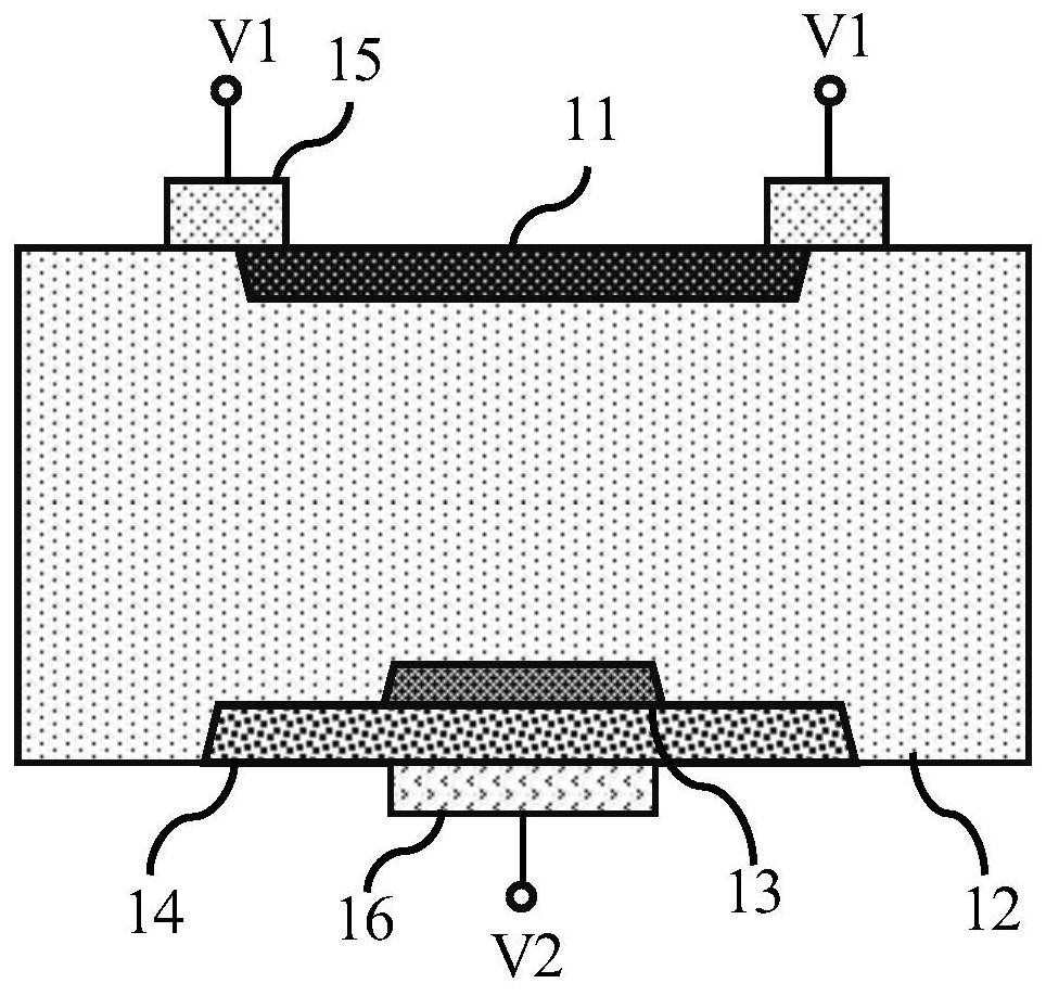
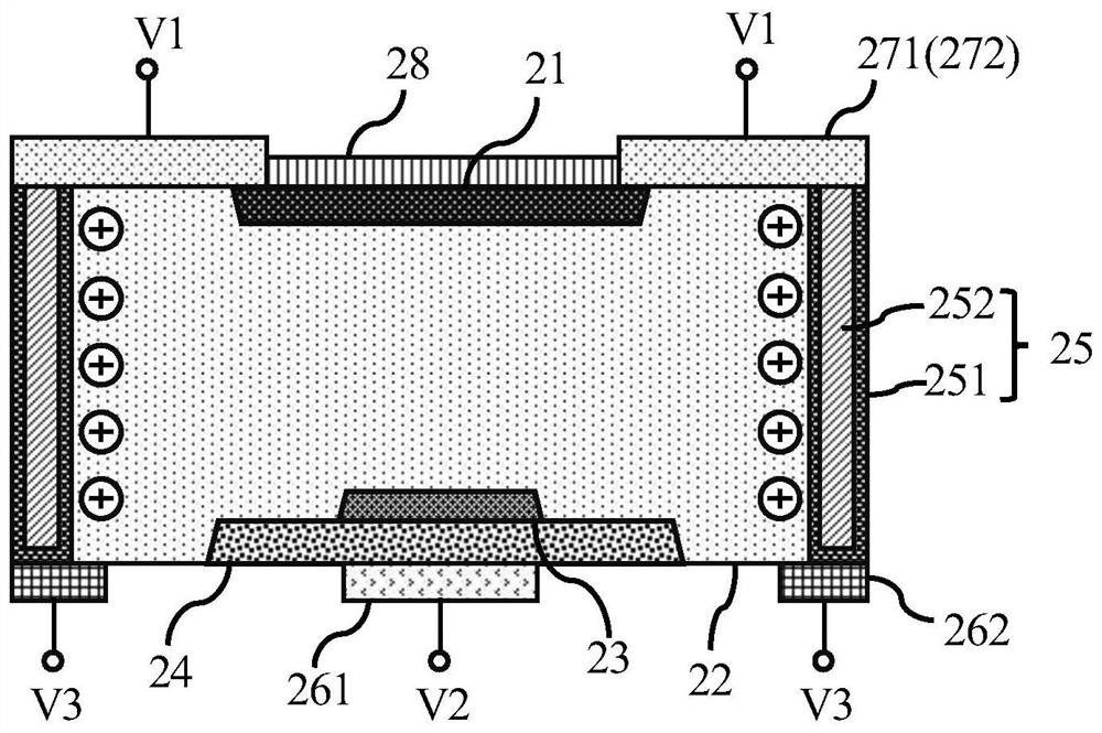
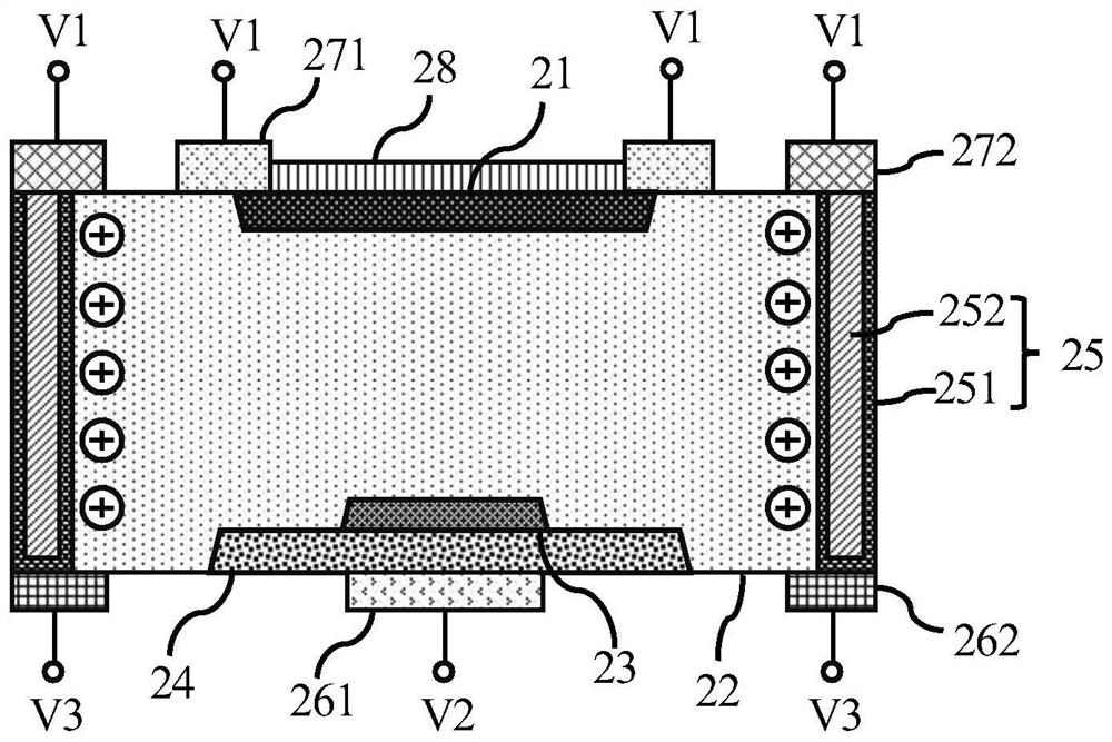
[0043] In order to make the objects, advantages and features of the present invention clearer, the following are combined with the appendix Figure 2a ~ Figure 4 The semiconductor device and its manufacturing method proposed by the present invention will be further described in detail. It should be noted that, the accompanying drawings are all in a very simplified form and in inaccurate scales, and are only used to facilitate and clearly assist the purpose of explaining the embodiments of the present invention.

[0044] An embodiment of the present invention provides a semiconductor device, the semiconductor device includes a substrate, an ion-doped region, an electric deep trench isolation ring, a top electrode and a bottom electrode, and the ion-doped region is formed on the substrate in; the deep trench isolation ring is formed in the substrate and surrounds the outer side of the ion-doped region, and is insulated from the ion-doped region in the substrate; the top electrod...


PUM


Abstract

The invention provides a semiconductor device and a manufacturing method thereof. The semiconductor device includes: a substrate; an ion-doped region formed in the substrate; an electrically deep trench isolation ring formed in the substrate and Surrounding the outside of the ion-doped region and insulated from the ion-doped region in the substrate; and a top electrode and a bottom electrode, the top electrode being formed on the top surface of the substrate and electrically connected to the top surface of the electrical deep trench isolation ring, the bottom electrode is formed on the bottom surface of the substrate and connected to the bottom surface of the electrical deep trench isolation ring, and the top electrode and The non-zero potential difference between the bottom electrodes can charge the electric deep trench isolation ring to change the charge distribution in the ion-doped region. The technical scheme of the invention can realize precise control of the ion doping concentration and depth in the ion doping region, thereby meeting the high requirements of advanced semiconductor devices.

Description

technical field [0001] The invention relates to the field of semiconductor integrated circuit manufacturing, in particular to a semiconductor device and a manufacturing method thereof. Background technique [0002] Photodiodes in semiconductor devices are based on an ion implantation process in which different types and concentrations of ions are implanted in different regions of the silicon substrate. Take Photon Avalanche Diode (PAD) as an example, see figure 1 , figure 1 is a schematic diagram of an existing semiconductor device containing an avalanche photodiode, from figure 1 It can be seen from the ion implantation process that the P-type ion heavily doped region 11, the intrinsic ion doped region 12, the P-type ion lightly doped region 13 and the N-type ion doped region 11 are formed in the silicon substrate from top to bottom. ion heavily doped region 14; and a negative electrode 15 is formed on the top surface of the P-type ion heavily doped region 11, and a posi...

Claims


Application Information

Patent Timeline
Patent Type & Authority Patents(China)
IPC IPC(8): H01L31/107H01L31/0352H01L31/0216H01L31/18
CPCH01L31/107H01L31/035272H01L31/035281H01L31/02161H01L31/1876Y02P70/50
Inventor 杨帆胡胜
Owner WUHAN XINXIN SEMICON MFG CO LTD
Why Eureka
Try Eureka