Semiconductor light emitting device

A technology of light-emitting devices and semiconductors, applied in semiconductor devices, electrical components, circuits, etc., can solve the problems of poor brightness improvement of light-emitting diodes, etc., and achieve the effects of improving luminous efficiency and current diffusion

Active Publication Date: 2020-08-11
KAISTAR LIGHTING (XIAMEN) CO LTD
View PDF13 Cites 0 Cited by
  • Summary
  • Abstract
  • Description
  • Claims
  • Application Information

AI Technical Summary

Problems solved by technology

However, the existing light-emitting diode structure has an area where the current is too concentrated, resulting in a poor effect of improving the brightness of the light-emitting diode.

Method used


Image

  • Semiconductor light emitting device
  • Semiconductor light emitting device
  • Semiconductor light emitting device

Examples


no. 1 example

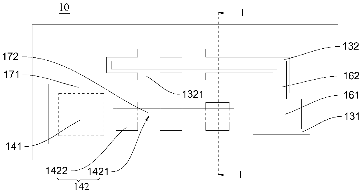
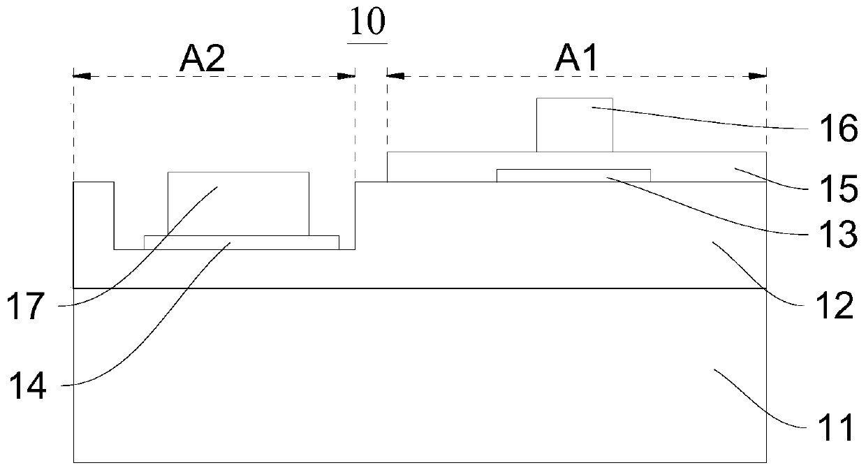
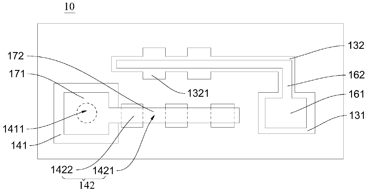
[0028] see Figure 1a and Figure 1b , the first embodiment of the present invention discloses a semiconductor light emitting device such as a light emitting diode (LED). like Figure 1a and 1b As shown, the semiconductor light emitting device 10 includes, for example: a substrate 11 , an epitaxial layer structure 12 , a current blocking layer 13 , a current blocking layer 14 , a current spreading layer 15 , an electrode 16 and an electrode 17 .

[0029] Specifically, such as Figure 1b As shown, the epitaxial layer structure 12 is disposed on the substrate 11 and includes a region A1 and a region A2. The current blocking layer 13 is disposed on the epitaxial layer structure 12 and located in the region A1. The current blocking layer 14 is disposed on the epitaxial layer structure 12 and located in the area A2. The current spreading layer 15 is disposed on the epitaxial layer structure 12 and located in the area A1 , wherein the current spreading layer 15 covers the curren...

no. 2 example

[0043] see Figure 2a and 2b , the second embodiment of the present invention discloses a semiconductor light emitting device. like Figure 2a and 2b As shown, the semiconductor light emitting device 20 is similar to the semiconductor light emitting device 10, and the semiconductor light emitting device 20 includes, for example: a substrate 21, an epitaxial layer structure 22, a current blocking layer 23, a current blocking layer 24, a current spreading layer 25, an electrode 26 and an electrode 27.

[0044] Specifically, such as Figure 2b As shown, the epitaxial layer structure 22 is disposed on the substrate 21 and includes a region A1 and a region A2. The current blocking layer 23 is disposed on the epitaxial layer structure 22 and located in the region A1. The current blocking layer 24 is disposed on the epitaxial layer structure 22 and located in the area A2. The current spreading layer 25 is disposed on the epitaxial layer structure 22 and located in the area A1 ,...

no. 3 example

[0050] see Figure 3a and Figure 3b , The third embodiment of the present invention provides a semiconductor light emitting device. like Figure 3a and Figure 3b As shown, the semiconductor light emitting device 30 is similar to the semiconductor light emitting device 10 , for example including: a substrate 31 , an epitaxial layer structure 32 , a current blocking layer 33 , a current blocking layer 34 , a current spreading layer 35 , an electrode 36 and an electrode 37 .

[0051] Specifically, such as Figure 3b As shown, the epitaxial layer structure 32 is disposed on the substrate 31 and includes a region A1 and a region A2. The current blocking layer 33 is disposed on the epitaxial layer structure 32 and located in the region A1. The current blocking layer 34 is disposed on the epitaxial layer structure 32 and located in the region A2. The current spreading layer 35 is disposed on the epitaxial layer structure 32 and located in the area A1 , wherein the current spr...


PUM

PropertyMeasurementUnit
transmittivityaaaaaaaaaa

Abstract

The present invention discloses a semiconductor light emitting device which includes: a substrate; an epitaxial layer structure disposed on the substrate; a first current blocking layer which is arranged on the epitaxial layer structure; a second current blocking layer which is arranged on the epitaxial layer structure; a current diffusion layer which is arranged on the epitaxial layer structure and covers the first current blocking layer; a first electrode which is arranged on one side, away from the epitaxial layer structure, of the current diffusion layer; and a second electrode which is arranged on the epitaxial layer structure and covers the second current blocking layer, wherein the first current blocking layer comprises a first main body blocking part and a first extension blockingpart, the second current blocking layer comprises a second main body blocking part and a second extension blocking part, the second extension blocking part comprises a plurality of conductive gaps, the first extension blocking part is provided with a plurality of first projection structures, and the plurality of first projection structures and the plurality of conductive gaps are arranged in an aligned manner. The current diffusion of the semiconductor light-emitting device can be improved, and the light-emitting efficiency is improved.

Description

technical field [0001] The invention relates to the technical field of semiconductors, in particular to a semiconductor light emitting device. Background technique [0002] With the continuous development of the LED industry, the cost-effective advantages of LED products have become increasingly prominent. The current light-emitting diode (LED) is provided with a current blocking layer under the P-type electrode to block the passage of current, that is, when the current is introduced by the P-type electrode, the current blocking layer can block the passage of current, thereby forcing the current to bypass the current blocking layer. The transparent conductive layer is diffused to enhance the brightness of the LED. However, there are areas where the current is too concentrated in the existing light emitting diode structure, resulting in poor effect of improving the brightness of the light emitting diode. Contents of the invention [0003] The invention provides a semicond...

Claims


Application Information

Patent Timeline
Patent Type & Authority Applications(China)
IPC IPC(8): H01L33/14H01L33/44H01L33/38
CPCH01L33/145H01L33/44H01L33/38H01L33/40
Inventor 卢宗宏
Owner KAISTAR LIGHTING (XIAMEN) CO LTD
Why Eureka
Try Eureka