Semiconductor device package

a technology of semiconductor devices and devices, applied in semiconductor devices, semiconductor/solid-state device details, electrical apparatus, etc., can solve the problems of optical interference, difficult to improve a contrast ratio, etc., and achieve the effect of improving current spreading, improving contrast ratio, and easy to understand

Pending Publication Date: 2021-02-11
SUZHOU LEKIN SEMICON CO LTD
View PDF1 Cites 1 Cited by
  • Summary
  • Abstract
  • Description
  • Claims
  • Application Information

AI Technical Summary

Benefits of technology

[0038]According to embodiments, it is possible to implement a semiconductor device package having an improved contrast ratio.
[0039]In addition, it is possible to manufacture a semiconductor device package having improved current spreading.

Problems solved by technology

In this case, in order to make the plurality of chips appear as one light source, a distance between the chips should be minimized, but problems such as optical interference may occur.
In addition, since a plurality of small-sized chips are disposed, there is a problem in that improving a contrast ratio is difficult when on / off-control is performed for each chip.

Method used


Image

  • Semiconductor device package
  • Semiconductor device package
  • Semiconductor device package

Examples


first embodiment

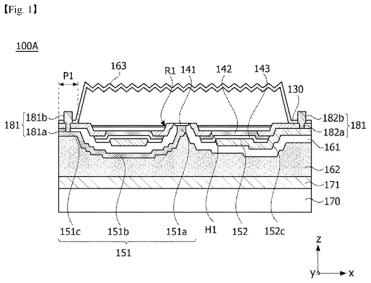
[0074]FIG. 1 is a cross-sectional view of a semiconductor device package according to a

[0075]Referring to FIG. 1, a semiconductor device package 100A according to the first embodiment may include a substrate 170 and a plurality of semiconductor structures 120 disposed to be spaced apart from each other.

[0076]The semiconductor device package 100A may further include a bonding layer 171, a channel layer 130, a first electrode 141, a second electrode 142, a reflective layer 143, a first interconnection line 151, a second interconnection line 152, a first insulating layer 161, a second insulating layer 162, a passivation layer 163, a first pad 181, and a second pad 182.

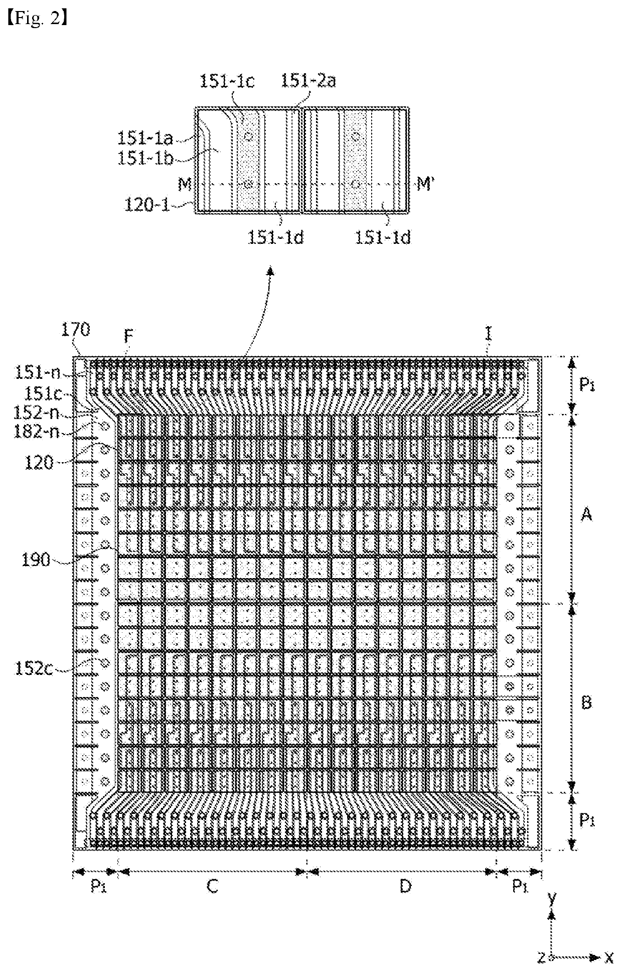
[0077]Here, it will be described below that FIG. 1 illustrates one semiconductor structure 120 disposed between the first pad 181 and the second pad 182 for convenience of description. However, as shown in FIG. 2, substantially, a plurality of semiconductor structures 120 (see FIG. 1) may be disposed to be spaced apart fr...

second embodiment

[0182]FIG. 10 is a sectional view of a semiconductor device package according to a

[0183]A semiconductor device package 100B according to the second embodiment may include the substrate 170, the plurality of semiconductor structures 120, the bonding layer 171, the channel layer 130, the first electrode 141, the second electrode 142, the reflective layer 143, the first interconnection line 151, the second interconnection line 152, the first insulating layer 161, the second insulating layer 162, the passivation layer 163, the first pad 181, and the second pad 182 which have been described with reference to FIG. 1, and the above-described contents may be equally applied.

[0184]However, an upper surface 121b of a first conductivity-type semiconductor layer 121 may include a first surface 121b-1, a second surface 121b-2 disposed below the first surface 121b-1, and an inclined surface 121b-3 positioned between the first surface 121b-1 and the second surface 121b-2. In addition, a plurality ...

third embodiment

[0190]Referring to FIG. 11, a semiconductor device package 100C may include a substrate 170, a plurality of semiconductor structures 120 disposed to be spaced apart from each other, and intermediate layers 164 disposed on side surfaces of the semiconductor structures 120.

[0191]In addition, the descriptions of the bonding layer 171, the channel layer 130, the first electrode 141, the second electrode 142, the reflective layer 143, the first interconnection line 151, the second interconnection line 152, the first insulating layer 161, the second insulating layer 162, the passivation layer 163, the first pad 181, and the second pad 182, which have been described in the semiconductor device package according to the first embodiment, may be equally applied to the semiconductor device package 100C according to the third embodiment. Therefore, detailed descriptions thereof will be omitted. In addition, when the bonding layer 171, the channel layer 130, the first electrode 141, the second ...


PUM

PropertyMeasurementUnit
sizeaaaaaaaaaa
lengthaaaaaaaaaa
sizeaaaaaaaaaa

Abstract

Disclosed in an embodiment is a semiconductor device package comprising a substrate and a plurality of semiconductor structures arranged to be spaced apart at the center of the substrate, wherein the semiconductor structure is arranged on the substrate and includes a first conductive type semiconductor layer, a second conductive type semiconductor layer, and an active layer arranged between the first conductive type semiconductor layer and the second conductive type semiconductor layer, and the ratio of the maximum height of the outermost surface of the first conductive type semiconductor layer to the length of the spacing distance between the adjacent semiconductor structures is 1:3 to 1:60.

Description

TECHNICAL FIELD[0001]The present invention relates to a semiconductor device package.BACKGROUND ART[0002]Semiconductor devices including compounds such as GaN and AlGaN may be variously used as light-emitting devices, light-receiving devices, and various diodes due to many advantages thereof, such as wide and easily adjustable bandgap energy.[0003]In particular, light-emitting devices, such as light-emitting diodes and laser diodes, which use a III-V group or II-VI group compound semiconductor material, are capable of rendering various colors, such as red, green, and blue, and ultraviolet rays by virtue of the development of thin-film growth technologies and device materials, are capable of producing white light at high efficiency using fluorescent materials or through color mixing, and have advantages such as low power consumption, semi-permanent lifespan, fast response speed, safety, and environmental friendliness as compared with conventional light sources such as fluorescent lam...

Claims


Application Information

Patent Timeline
Patent Type & Authority Applications(United States)
IPC IPC(8): H01L23/538H01L25/075H01L33/62
CPCH01L23/5386H01L33/62H01L25/075H01L25/065H01L23/485H01L33/22H01L33/387H01L27/156
Inventor LEE, SANG YOULKANG, KI MANLEE, EUN DK
Owner SUZHOU LEKIN SEMICON CO LTD
Why Eureka
Try Eureka