Semiconductor light-emitting element and light-emitting device

A technology for light-emitting elements and semiconductors, applied in semiconductor devices, electrical components, circuits, etc., can solve problems such as electrode shading, and achieve the effects of reducing shading, simple process, and improving uniform dispersion of light.

Active Publication Date: 2020-05-15
TIANJIN SANAN OPTOELECTRONICS
View PDF3 Cites 0 Cited by
  • Summary
  • Abstract
  • Description
  • Claims
  • Application Information

AI Technical Summary

Problems solved by technology

However, after substrate transfer, the N-type epitaxial layer is reversed upwards, and it is necessary to design a contact layer and an electrode layer on the N-type GaAs epitaxial layer, which will cause the problem of electrode shading

Method used


Image

  • Semiconductor light-emitting element and light-emitting device
  • Semiconductor light-emitting element and light-emitting device
  • Semiconductor light-emitting element and light-emitting device

Examples


Embodiment 1

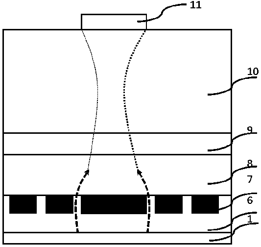
[0067] Such as figure 1 Shown is a traditional semiconductor light emitting element as described in the background art, including:

[0068] A semiconductor light emitting sequence, the semiconductor light emitting sequence includes a first conductivity type semiconductor layer 10, a light emitting layer 9 and a second conductivity type semiconductor layer 8;

[0069] A partial area on one side of the second conductivity type semiconductor layer 8 is covered by the electrical insulating layer 7 to form an electrical contact area, and a partial area on one side not covered by the electrical insulating layer 7 is an electrical contact area. The electrically insulating layer is usually silicon oxide or silicon nitride or calcium fluoride or magnesium fluoride. A plurality of openings are usually formed on the electrical insulating layer, and electrical contact areas are located within the openings.

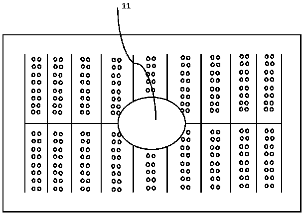
[0070] The first electrode 11, including the main pad electrode (generally circ...

Embodiment 2

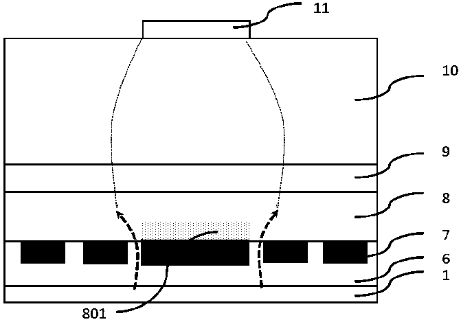
[0127] Such as Figure 13 As shown, in this embodiment, an alternative implementation is provided, specifically providing the following semiconductor light-emitting element, which includes a semiconductor light-emitting sequence, and the semiconductor light-emitting sequence includes a first conductivity type semiconductor layer 10, a light-emitting layer 9 and a second conductivity type semiconductor layer 8;

[0128] The electrical insulating layer 7 on the side of the second conductive type semiconductor layer 8 has multiple openings, and one side of the second conductive type semiconductor layer is set as an electrical contact area and an electrical insulating area.

[0129] The opening is filled with ohmic contact blocks 14, and there are many ohmic contact blocks 14, but they are not formed under the main pad electrode for injecting current outside the first electrode. The shape of the ohmic contact block 14 is block, and the metal material is at least one of gold germa...

Embodiment 3

[0149] Such as Figure 22 As shown, in this embodiment, another semiconductor light emitting element is provided, and the semiconductor light emitting sequence includes a first conductivity type semiconductor layer 10, a light emitting layer 9 and a second conductivity type semiconductor layer 8;

[0150] The side of the second conductivity type semiconductor layer 8 includes an electrical insulating layer, the fluoride electrical insulating layer has multiple openings, and one side of the second conductivity type semiconductor layer is set as an electrical contact area and an electrical insulation area.

[0151] The openings are filled with ohmic contact blocks or ohmic contact layers.

[0152] The electrical insulating layer is fluoride, specifically at least one of magnesium fluoride and calcium fluoride.

[0153] The fluorine ions of the fluoride diffuse into the second conductivity type semiconductor layer to form a current blocking region.

[0154] The first electrode ...


PUM

PropertyMeasurementUnit
thicknessaaaaaaaaaa
thicknessaaaaaaaaaa
thicknessaaaaaaaaaa

Abstract

A semiconductor light emitting element includes a semiconductor light emitting sequence including a first conductivity type semiconductor layer, a light emitting layer and a second conductivity type semiconductor layer, wherein the electric insulation layer covers a partial region at one side of the second conductive type semiconductor layer to form an electric insulation region, an uncovered partial region at one side of the second conductive type semiconductor layer is an electric contact region, and the second conductive type semiconductor layer comprises a fluorine-containing region; the electric insulation layer is fluoride, the fluorine ions of the fluoride enter the second conductive type semiconductor layer through high-temperature diffusion to form a fluorine-containing region, and the fluorine-containing region is formed at least in the second conductivity-type semiconductor layer below the main pad electrode of the first electrode. According to the invention, the local square resistance can be improved, the current dispersion condition in the second conductive type semiconductor layer below the main bonding pad electrode of the first electrode is improved, and the current is promoted to transversely diffuse to the surrounding area of the main bonding pad electrode far away from the first electrode, so that the light uniform dispersion is improved.

Description

technical field [0001] The invention relates to an LED light-emitting element. Background technique [0002] At present, LED light-emitting components have been widely used in equipment in many fields such as lighting, display, traffic signal, data storage, and medical equipment. There are many factors affecting the light efficiency of LED light-emitting elements, including the internal quantum efficiency of the epitaxial structure, the heat dissipation of the substrate, the light output efficiency of the light output side, and so on. [0003] In order to improve the heat dissipation of the substrate, on the one hand, the epitaxial growth substrate can be replaced with a substrate with higher thermal conductivity, because the thermal conductivity of silicon or silicon carbide or metal substrates is higher than that of gallium arsenide. The combination process realizes substrate transfer to silicon or silicon carbide or metal substrates. However, after substrate transfer, t...

Claims


Application Information

Patent Timeline
Patent Type & Authority Applications(China)
IPC IPC(8): H01L33/14H01L33/00
CPCH01L33/145H01L33/0062
Inventor 张东炎吴俊毅刘文王晶郭桓邵李慧文王笃祥
Owner TIANJIN SANAN OPTOELECTRONICS
Why Eureka
Try Eureka