Light-emission device and its manufacturing method

A technology of light emitters and emitters, which is applied in semiconductor/solid-state device manufacturing, instruments, light sources, etc., and can solve problems such as deterioration of screen clarity and display dysfunction.

Inactive Publication Date: 2006-06-14
SANYO ELECTRIC CO LTD
View PDF0 Cites 0 Cited by
  • Summary
  • Abstract
  • Description
  • Claims
  • Application Information

AI Technical Summary

Problems solved by technology

When poor luminescence occurs for any reason, non-luminous areas appear on the

Method used


Image

  • Light-emission device and its manufacturing method
  • Light-emission device and its manufacturing method
  • Light-emission device and its manufacturing method

Examples


Embodiment Construction

[0016] The present invention will now be described in terms of preferred embodiments, which are not intended to limit the scope of the invention but to illustrate the invention. All features and combinations thereof described in the embodiments are not necessarily essential to the invention.

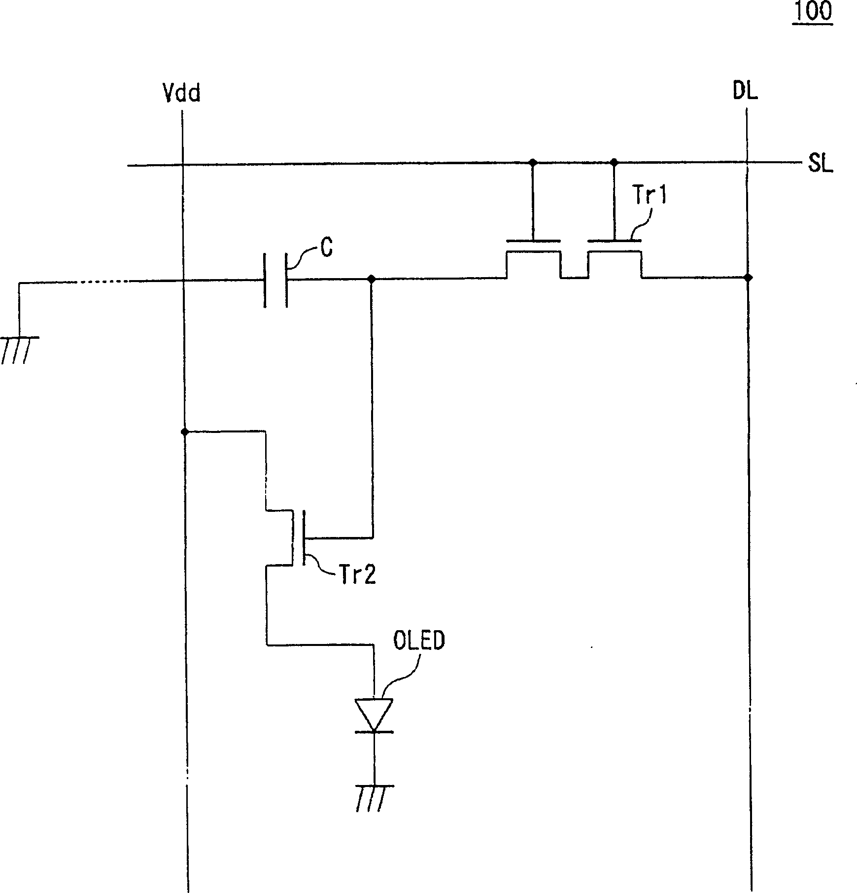
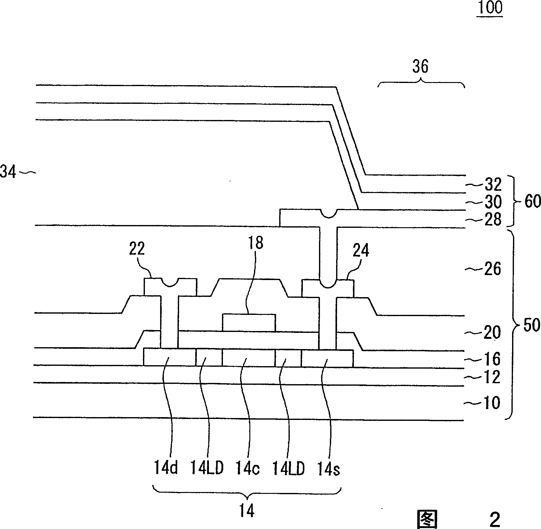
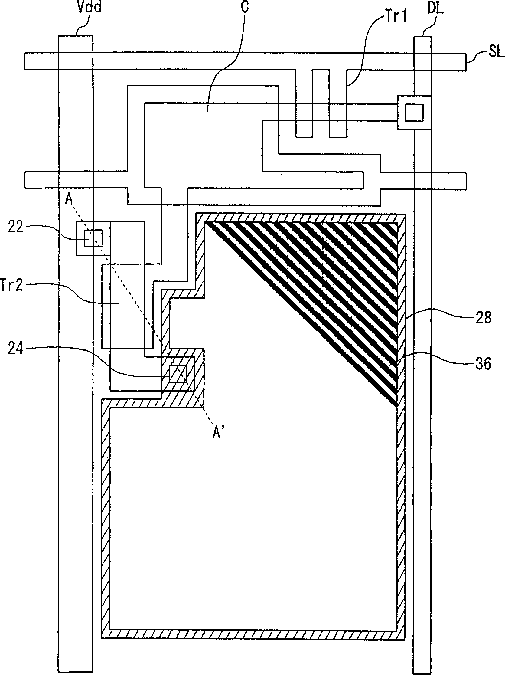
[0017] figure 1 is a circuit structure of a single pixel of the light emitter 100 of an embodiment. The circuit includes an organic light emitting element OLED, two transistors Tr for controlling the organic light emitting element OLED 1 and Tr 2 , a capacitor C, a scanning line SL for transmitting scanning signals, a data line DL for transmitting brightness data, and a power supply line Vdd for providing electric power.

[0018] The power line Vdd provides electric power to make the organic light emitting element OLED emit light. The data line DL transmits the set brightness data to the second transistor Tr 2 (hereinafter also referred to as "driving transistor"). The scan line SL...


PUM


Abstract

An organic EL device manufactured by a new method to reduce the occurrence of undesirable light emission in the organic EL device. The pixel aperture is formed on a portion other than a portion above a contact hole connecting the source of the driving transistor and the pixel electrode of the organic light emitting device. The uneven portion of the pixel electrode is covered by an insulating layer to avoid short circuit between the pixel electrode and the opposite electrode.

Description

technical field [0001] The present invention relates to light emitters and methods of manufacturing light emitters, and more particularly to techniques for reducing the number of occurrences of undesirable lighting of light emitters. Background technique [0002] Organic electroluminescent displays (hereinafter also referred to as "organic EL displays" or "organic EL panels") are attracting attention as a new flat-type display. In particular, active matrix type organic EL displays having thin film transistors (hereinafter referred to as "TFTS") as switching elements are expected to replace currently popular liquid crystal displays in the near future, and are being rapidly developed in practical use. [0003] Unlike liquid crystal displays, organic EL displays have self-emitting devices. This eliminates the need for an essential backlight for liquid crystal displays, making the device compact and lightweight. Furthermore, the organic EL panel can be expected to be used as a...

Claims


Application Information

Patent Timeline
IPC IPC(8): H05B33/10H05B33/14G09G3/30G09F9/30H01L27/32H01L51/50H05B33/22
CPCH10K59/122H05B33/26
Inventor 野口幸宏土屋博佐野景一
Owner SANYO ELECTRIC CO LTD
Why Eureka
Try Eureka