Depletion mode high electron mobility field effect transistor (HEMT) semiconductor device having beryllium doped Schottky contact layers

a technology of hemt and schottky, which is applied in the direction of semiconductor devices, electrical equipment, basic electric elements, etc., can solve the problems of future growths at risk of increased levels of magnesium background impurity incorporation, unstable operation of fets, and mis approach, and achieves efficient creation of acceptor level states in gan, enhance schottky barrier height, and enhance the effect of schottky

Active Publication Date: 2022-06-14
RAYTHEON CO
View PDF58 Cites 0 Cited by
  • Summary
  • Abstract
  • Description
  • Claims
  • Application Information

AI Technical Summary

Benefits of technology

[0011]Further, the inventors have recognized that beryllium doping in GaN by MBE is possible up to 5×10¹⁹ / cm3 without creating additional defects and disorder in the material and eventually lead to structural degradation. Doping levels below 1×10¹⁶ / cm3 become inefficient at shifting the band structure to realize enhanced Schottky barrier heights. Further, the vapor pressure of beryllium is such that beryllium produces no undesired background doping or chamber memory effects occur following its use for MBE growth. The inventors have experimentally found that 25 nm capping layers of 5×10¹⁸ / cm3 beryllium doped GaN grown by MBE on certain depletion mode AlGaN / GaN HEMTs can modified the band structure to produce enhancement mode HEMTs suggesting beryllium doping can efficiently create acceptor level states in GaN.
[0012]The inventors have recognized that beryllium as used as an acceptor level dopant for GaN (Be:GaN) is stable at high temperature, for example, up to at least 900 degrees Celcius, in both growth and processing steps. The resistivity of GaN layers with beryllium dopants increases, which is different from magnesium doped GaN wherein the resistivity decreases and p-type conductivity is observed. This beryllium doped GaN provides an excellent material for increasing the effective Schottky barrier height for diodes and FETs by growing a beryllium doped Group III-Nitride cap layer 1 nm to 10 nm in thickness on top of Group III-Nitride material structures for diodes and FETs. The beryllium doped cap layer increases the Schottky barrier height. The increased barrier height provides many benefits, including: 1. reducing gate leakage current; 2. increasing breakdown voltage; and 3. enhancing the reliability of diodes and FETs. In addition, this layer is used as surface passivation to improve current dispersion in RF devices.
[0013]Still further, the inventors have recognized that the addition of the doped Group III-Nitride cap layer on the surface of the Group III-Nitride HEMT does not contribute to increasing the polarization induced charge in the 2DEG of the Group III-Nitride HEMT. The Group III-Nitride HEMT is formed from a pair of stacked Group III-Nitride layers. A lower one of the pair of stacked Group III-Nitride layers is a channel layer and an upper one of the pair of stacked Group III-Nitride layers is a barrier layer. A pair of stacked Group III-Nitride layers form a heterojunction and a polarization mismatch at the heterojunction interface results in the formation of 2DEG in the channel layer. The barrier layer can be formed by one or more Group III-Nitride layers, such that the Group III-Nitride layers in the barrier layer contribute in some way to establishing the polarization mismatch at the heterojunction. The Group III-Nitride cap layer can be one or more Group III-Nitride semiconducting layers directly in contact with the barrier layer. The materials in the Group III-Nitride cap layer do not contribute to an increase in the polarization mismatch like the Group III-Nitride materials in the barrier layer, rather the Group III-Nitride cap layer materials improve surface passivation, leakage, and dispersion.

Problems solved by technology

This MIS approach has an issue with surface states between the insulator films and semiconductor.
More particularly, these surface states trap carriers and cause an unstable operation of FETs.
While magnesium doped p-type GaN capped devices have been reported, the use of magnesium creates a memory effect in deposition systems that puts future growths at risk for increased levels of magnesium background impurity incorporation.

Method used


Image

  • Depletion mode high electron mobility field effect transistor (HEMT) semiconductor device having beryllium doped Schottky contact layers
  • Depletion mode high electron mobility field effect transistor (HEMT) semiconductor device having beryllium doped Schottky contact layers

Examples


Embodiment Construction

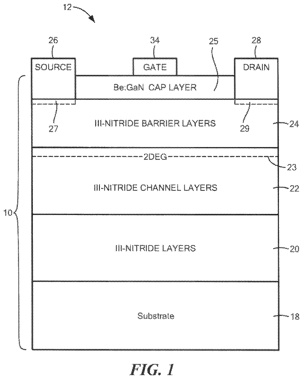
[0020]Referring now to FIG. 1, a semiconductor structure 10 is shown having a depletion mode (D-mode) field effect transistor 12, here a D-mode HEMT. The D-mode HEMT 12 includes a source electrode 26, a drain electrode 28 and a gate electrode 34 disposed between the source electrode 26 and the drain electrode 28, as shown.

[0021]More particularly, the semiconductor structure 10 includes a single crystal substrate 18, here for example silicon carbide (SiC), and an epitaxially grown Group III-Nitride structure, here a stack of epitaxially grown Group III-Nitride structure semiconductor layers 20, 22, 24; layer 20 being one or more epitaxial grown Group III-Nitride materials forming nucleation and buffer regions of a HEMT structure, layer 22 being epitaxially grown undoped Group III-Nitride channel material with lower resistivity than the layer 20 materials, here for example GaN, and layer 24 being one or more epitaxial grown Group III-Nitride barrier materials, here for example AlGaN. ...


PUM

PropertyMeasurementUnit
thicknessaaaaaaaaaa
thicknessaaaaaaaaaa
thicknessaaaaaaaaaa

Abstract

A semiconductor device having a substrate, a pair of Group III-Nitride layers on the substrate forming: a heterojunction with a 2 Dimensional Electron Gas (2DEG) channel in a lower one of the pair of Group III-Nitride layers, a cap beryllium doped Group III-Nitride layer on the upper one of the pair of Group III-Nitride layers; and an electrical contact in Schottky contact with a portion of the cap beryllium doped, Group III-Nitride layer.

Description

TECHNICAL FIELD[0001]This disclosure relates generally to depletion mode High Electron Mobile Field Effect Transistor (HEMT) semiconductor devices and more particularly to depletion mode HEMT semiconductor devices having Schottky contact layers.BACKGROUND[0002]As is known in the art, active semiconductor devices such as for example, diodes and FETs (Field Effect Transistors) based on Group III-Nitride materials, such as GaN, AlGaN, InN, AlN, and ScAlN, have recently demonstrated excellent RF / Microwave performances, which are achieved with an optimization of material, process, device, and design technologies, see for example, GaN-Based Schottky Diode by Yaqi Wang, http: / / dx.doi.org / 10.5772 / intechopen.77024, Submitted: Nov. 27, 2017 Reviewed: Apr. 5, 2018 Published: Sep. 12, 2018.[0003]A prior attempt to increase Schottky barrier height for these semiconductor devices was to introduce a dielectric insulator, such as silicon nitride or oxide, aluminum nitride or oxide, and various othe...

Claims


Application Information

Patent Timeline
Patent Type & Authority Patents(United States)
IPC IPC(8): H01L29/20H01L29/205H01L29/778H01L29/47
CPCH01L29/475H01L29/2003H01L29/205H01L29/7786H01L29/207H01L29/41766H01L29/432
Inventor HWANG, KIUCHULSCHULTZ, BRIAN D.LOGAN, JOHNLEONI, ROBERT E.KOLIAS, NICHOLAS J.
Owner RAYTHEON CO
Why Eureka
Try Eureka