LED chip structure of ALD deposition current expansion layer and manufacturing method thereof

A technology of LED chip and current expansion layer, which is applied in circuits, electrical components, semiconductor devices, etc., can solve problems such as reducing light absorption, and achieve the effects of reducing leakage, improving optoelectronic performance, and uniform thickness

Pending Publication Date: 2021-03-19
普瑞(无锡)研发有限公司
View PDF0 Cites 0 Cited by
  • Summary
  • Abstract
  • Description
  • Claims
  • Application Information

AI Technical Summary

Problems solved by technology

[0003] The applicant aims at the defects of single ITO thin film in the prior art, and provides an LED chip structure and its manufacturing method of ALD deposited current spreading layer, which can improve the defects of single ITO film by using ITO, aluminum atoms and aluminum oxide composite conductive film , reduce the absorption of light, and at the same time facilitate the expansion of the current, increase the light angle of the chip, improve the uniformity and consistency of the deposited layer, and also protect the ITO film

Method used


Image

  • LED chip structure of ALD deposition current expansion layer and manufacturing method thereof

Examples


Embodiment Construction

[0022] The specific implementation manner of the present invention will be described below in conjunction with the accompanying drawings.

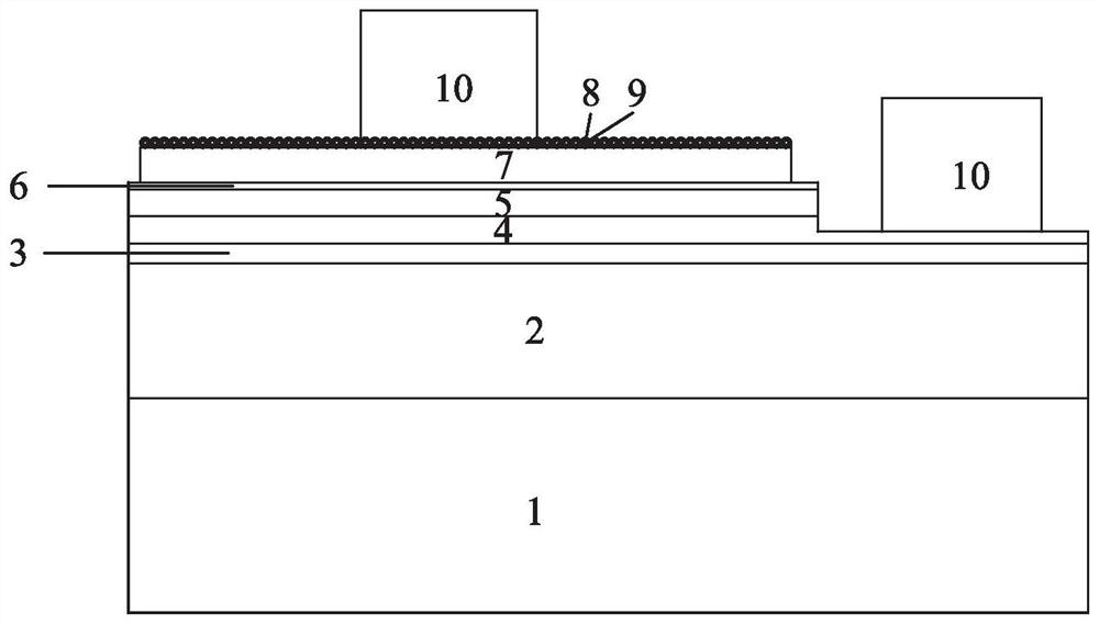
[0023] Such as figure 1 As shown, in the LED chip structure of the ALD deposition current spreading layer of the present invention, the LED chip epitaxial structure is grown on the chip substrate 1, and the chip substrate 1 includes but not limited to sapphire, silicon wafer, silicon carbide wafer or metal. For example, using MOCVD equipment (MOCVD, Metal-organic Chemical Vapor Deposition, Metal-Organic Compound Chemical Vapor Deposition) to grow an LED chip epitaxial structure on the chip substrate 1, the LED chip epitaxial structure is a multi-layer structure, depending on actual needs, for example, It is buffer layer 2, U-GaN layer 3, N-GaN layer 4, multi-quantum well layer 5 and P-GaN layer 6 grown in sequence, or N-GaN layer 4, multi-quantum well layer 5 and The P-GaN layer 6 , the LED chip epitaxial structure covers the entire surfa...


PUM

PropertyMeasurementUnit
thicknessaaaaaaaaaa

Abstract

The invention discloses an LED chip structure of an ALD deposition current expansion layer and a manufacturing method thereof, and the LED chip structure of the ALD deposition current expansion layercomprises the steps: growing an LED chip epitaxial structure on a chip substrate, manufacturing a transparent conductive layer on the LED chip epitaxial structure, and enabling the transparent conductive layer to comprise an ITO film which is plated through employing an electron beam evaporation technology, wherein the aluminum atom layer is plated by using an electron beam evaporation technology,the aluminum oxide film is deposited by using an ALD technology, and the core-shell structure film takes aluminum atoms as a core and aluminum oxide as a shell. On the basis of an ITO thin film, an aluminum atom layer is deposited firstly, then aluminum oxide is deposited through the ALD technology, a core-shell structure film with aluminum atoms as a core and aluminum oxide as a shell is formed,the aluminum oxide layer can reduce light absorption, current diffusion of the ITO thin film can be improved, the light emitting angle of a chip is increased, and the photoelectric performance of thechip is improved; and the effects of improving brightness and reducing voltage are achieved.

Description

technical field [0001] The invention relates to the technical field of semiconductors, in particular to an LED chip structure with an ALD deposited current spreading layer and a manufacturing method thereof. Background technique [0002] Light-emitting diode (LED) is a solid-state light-emitting device that converts electrical energy into light energy. Among them, GaN-based LED chips have been greatly developed and applied. The luminous efficiency of light-emitting diodes mainly has two factors: the internal quantum efficiency and external quantum efficiency of the device. At present, the internal quantum efficiency of GaN-based LEDs can reach more than 70%, and there is little room for further improvement. In order to improve the external quantum efficiency of the LED, the current spreading layer is used as the light-extracting layer, which directly affects the photoelectric performance of the LED. At present, ITO is usually used as the current spreading layer. The ITO fil...

Claims


Application Information

Patent Timeline
Patent Type & Authority Applications(China)
IPC IPC(8): H01L33/14H01L33/06H01L33/32H01L33/00
CPCH01L33/0075H01L33/06H01L33/14H01L33/32
Inventor 闫晓密
Owner 普瑞(无锡)研发有限公司
Why Eureka
Try Eureka