Semiconductor light emitting device

a technology of semiconductor film and light-emitting device, which is applied in the direction of semiconductor film, basic electric elements, electrical equipment, etc., can solve the problems of reducing light extraction efficiency, difficult to suppress the self-absorption of light propagating inside the semiconductor film without, and reducing the light extraction efficiency. , to achieve the effect of improving light extraction efficiency and suppressing the self-absorption of light propagating in the semiconductor film

Inactive Publication Date: 2013-01-15
STANLEY ELECTRIC CO LTD
View PDF6 Cites 1 Cited by
  • Summary
  • Abstract
  • Description
  • Claims
  • Application Information

AI Technical Summary

Benefits of technology

[0008]Although light is more likely to be extracted outside by forming the recesses / protrusions on the light-extraction-surface side, light multi-reflected inside the semiconductor film still exists. As mentioned above, in order to promote current spread in the semiconductor film, the thickness of the semiconductor film needs to be secured, but the greater the thickness of the semiconductor film is, the longer the propagation distance (optical path length) of light multi-reflected inside the semiconductor film is, which means that self-absorption is more likely to occur, thus reducing the light extraction efficiency. That is, it is difficult to suppress the self-absorption of light propagating inside the semiconductor film without hindering current spread inside the semiconductor film.
[0009]The present invention has been made in view of the above points, and an object thereof is to provide a semiconductor light emitting device which can suppress the self-absorption of light propagating inside the semiconductor film without hindering current spread inside the semiconductor film.
[0011]According to the semiconductor light emitting device of the present invention, the self-absorption of light propagating in the semiconductor film can be suppressed without hindering current spread therein, thus improving the light extraction efficiency.

Problems solved by technology

As mentioned above, in order to promote current spread in the semiconductor film, the thickness of the semiconductor film needs to be secured, but the greater the thickness of the semiconductor film is, the longer the propagation distance (optical path length) of light multi-reflected inside the semiconductor film is, which means that self-absorption is more likely to occur, thus reducing the light extraction efficiency.
That is, it is difficult to suppress the self-absorption of light propagating inside the semiconductor film without hindering current spread inside the semiconductor film.

Method used


Image

  • Semiconductor light emitting device
  • Semiconductor light emitting device
  • Semiconductor light emitting device

Examples


Embodiment Construction

[0028]Embodiments of the present invention will be described with reference to the accompanying drawings. In the figures cited below, the same reference numerals are used to denote substantially the same or equivalent constituents or parts.

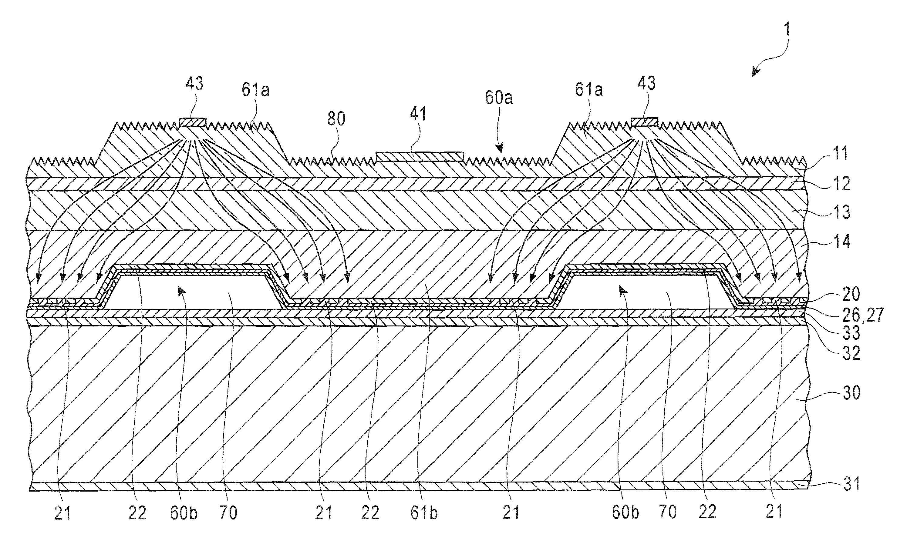
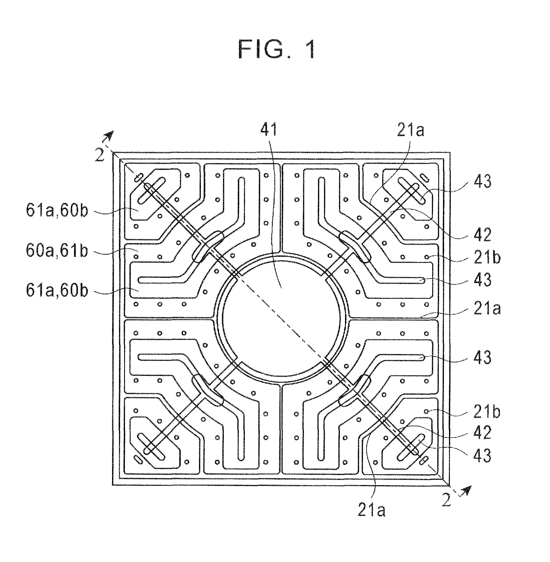
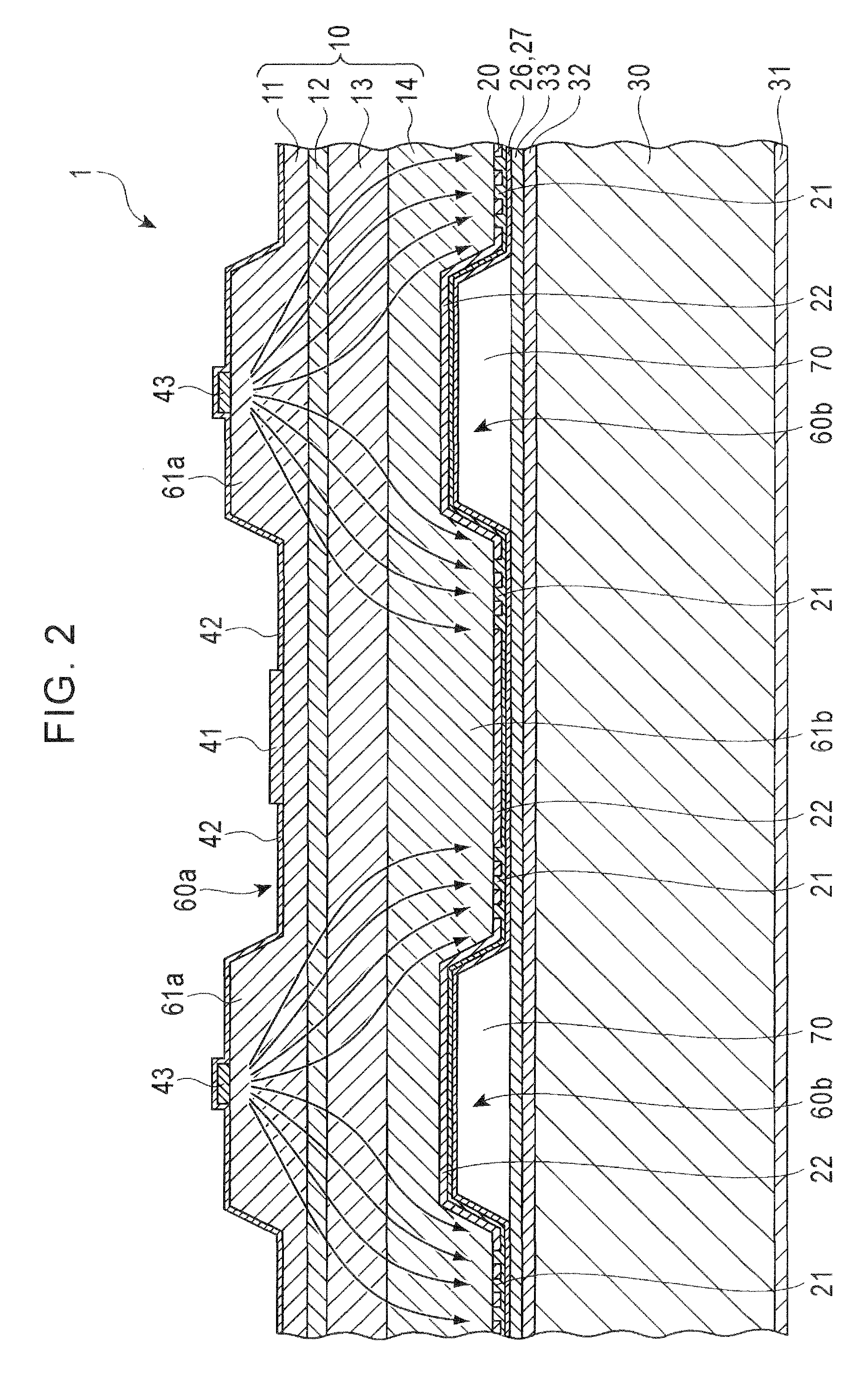
[0029]FIG. 1 is a plan view showing the configuration of a semiconductor light emitting device 1 according to an embodiment of the present invention, and FIG. 2 is a cross-sectional view taken along line 2-2 in FIG. 1.

[0030]The semiconductor light emitting device 1 has a so-called stuck-together structure where a semiconductor film 10 and a support substrate 30 are joined via a reflecting film 20. The semiconductor film 10 is configured with an n-type clad layer 11, a light emitting layer 12, a p-type clad layer 13, and a p-type contact layer 14 that are laid one over another in that order from the light-extraction-surface side. The total thickness of the semiconductor film 10 is, for example, 6 μm, and the outline of the principal surface is, for...


PUM


Abstract

A semiconductor light emitting device which can suppress the self-absorption of light propagating in a semiconductor film without hindering current spread therein. A reflecting film provided between a support substrate and the semiconductor film of the device includes reflecting electrodes that are in ohmic contact with the semiconductor film and that form current paths between the reflecting electrodes and surface electrodes in the semiconductor film. The reflecting electrodes are in contact with the semiconductor film at such positions that the surface electrodes, provided on the light-extraction-surface-side surface of the semiconductor film, are not over the reflecting electrodes along a direction of the thickness of the semiconductor film. The semiconductor film has reflecting-surface-side recesses made in regions containing regions directly under the surface electrodes and recessed toward the light-extraction-surface side, and reflecting-surface-side protrusions provided in regions containing parts of the semiconductor film in contact with the reflecting electrodes and bonded to the support substrate via the reflecting film.

Description

BACKGROUND OF THE INVENTION[0001]1. Field of the Invention[0002]The present invention relates to a semiconductor light emitting device such as an LED (light emitting diode) and particularly to a technique for improving light extraction efficiency.[0003]2. Description of the Related Art[0004]For LEDs formed of AlGaInP-based material, the band gap of the light emitting layer is larger than the band gap of a GaAs substrate used in crystal-growth. Hence, part of light directed toward the light-extraction-surface side out of the light emitted from the light emitting layer can be extracted, while light directed to the GaAs-substrate side is then absorbed by the GaAs substrate.[0005]Japanese Patent Kokai No. 2002-217450 (Patent Literature 1) discloses an LED which is produced by forming a semiconductor film made of AlGaInP-based material on a GaAs substrate, then sticking the semiconductor film to a support substrate via a reflecting film made of metal having high reflectance, and then rem...

Claims


Application Information

Patent Timeline
Patent Type & Authority Patents(United States)
IPC IPC(8): H01L33/00
CPCH01L33/20H01L33/46H01L33/0079H01L33/22H01L33/38H01L33/387H01L33/0093
Inventor KAZAMA, TAKUYA
Owner STANLEY ELECTRIC CO LTD
Why Eureka
Try Eureka