Gating device and preparation method thereof

A technology for a gated device and a growth method, which is applied in the field of gated devices and their preparation, can solve problems such as the application of gated devices that cannot be supported, threshold voltage fluctuations, etc., so as to reduce the number and distribution of defects, reduce threshold voltage fluctuations, reduce random effect

Active Publication Date: 2020-08-18
NAT UNIV OF DEFENSE TECH
View PDF5 Cites 1 Cited by
  • Summary
  • Abstract
  • Description
  • Claims
  • Application Information

AI Technical Summary

Problems solved by technology

[0005] The purpose of the present invention is to provide a gating device and its preparation method in order to solve the problem that the programmable metalli

Method used


Image

  • Gating device and preparation method thereof
  • Gating device and preparation method thereof
  • Gating device and preparation method thereof

Examples


Embodiment Construction

[0043] In order to make the purpose, technical solutions and advantages of the embodiments of the present invention clearer, the technical solutions in the embodiments of the present invention will be clearly and completely described below in conjunction with the drawings in the embodiments of the present invention. Obviously, the described embodiments It is a part of embodiments of the present invention, but not all embodiments.

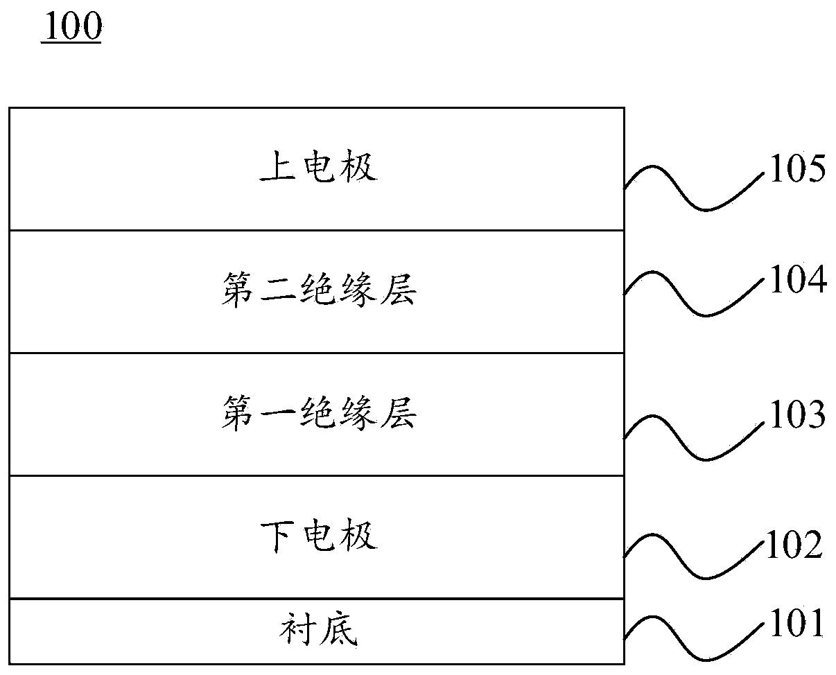
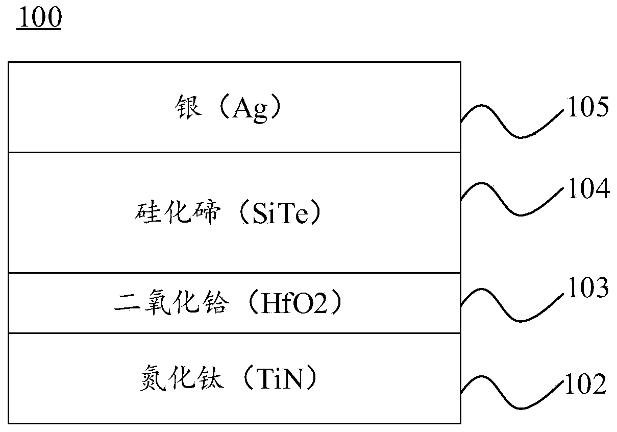
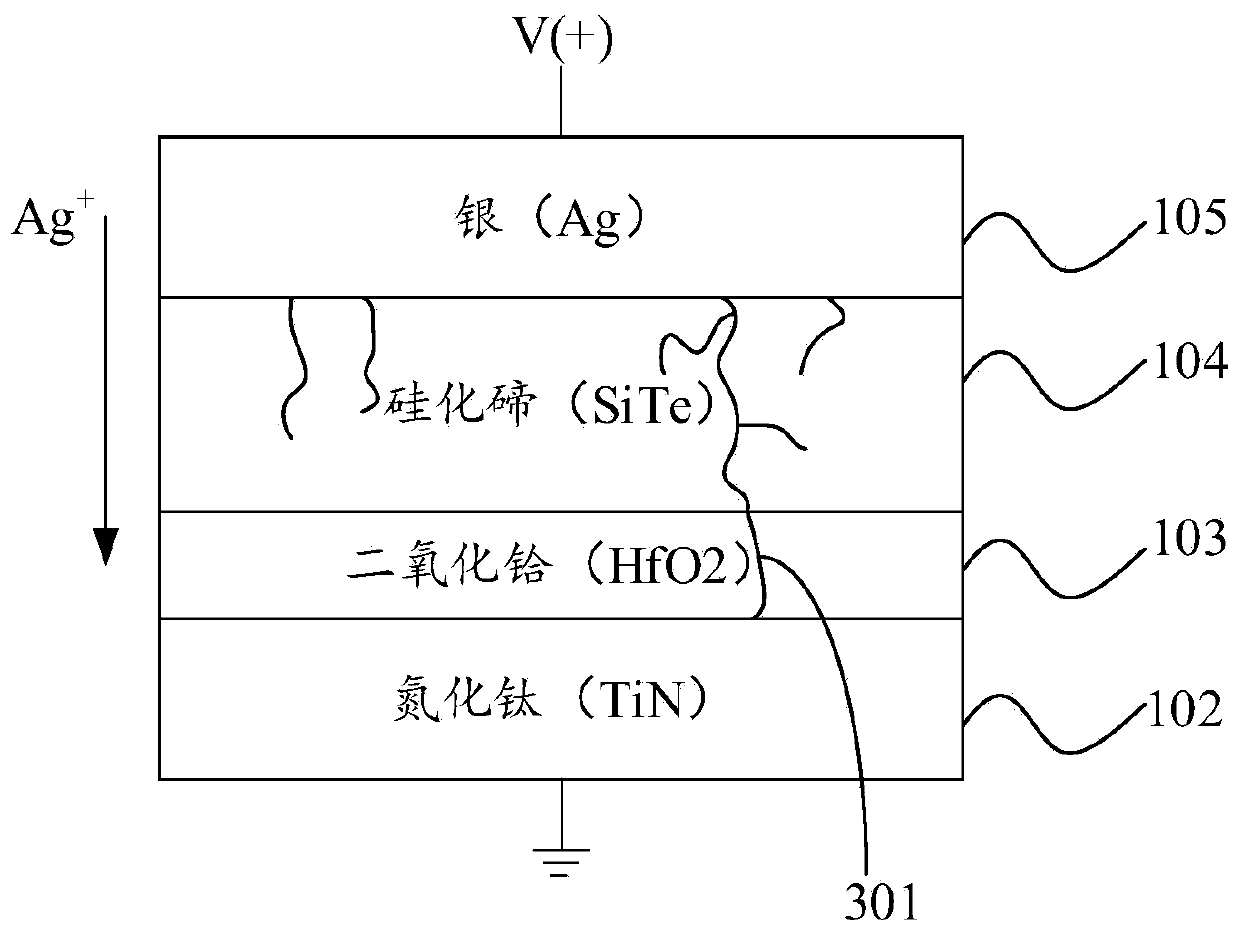
[0044] In the structure of the memristor cross array, in order to solve the problem of crosstalk current, the memristor and the gating device can be connected in series to form a 1S1R (one Selector one RRAM, a gating device and a memristor) memristive structure. The integration of the cross array, the memristive structure provided with the gating device can effectively reduce the leakage current generated by the unselected memristors in the memristor cross array, reduce the static power consumption, thereby improving the performance of the memristor ...


PUM


Abstract

The invention provides a gating device and a preparation method thereof, and relates to the technical field of micro-nano electronic devices. The gating device comprises a lower electrode, a first insulating layer, a second insulating layer and an upper electrode which are sequentially arranged on a substrate from bottom to top, wherein the lower electrode is an inert electrode, the upper electrode is an active electrode, and the metal ion mobility of the first insulating layer is smaller than that of the second insulating layer. According to the scheme of the invention, two insulating layerswith different metal ion mobility are arranged between the lower electrode and the upper electrode in the gating device, wherein the two insulating layers are the first insulating layer and the secondinsulating layer, and the metal ion mobility of the first insulating layer is smaller than that of the second insulating layer, so that the re-connection position of the conductive channel is controlled, the randomness of the position of the newly formed conductive channel is reduced, the fluctuation of the threshold voltage in different cyclic operations is effectively reduced, and the application of the gating device in a memristor cross array is effectively supported.

Description

technical field [0001] The invention relates to the technical field of micro-nano electronic devices, in particular to a gate device and a preparation method thereof. Background technique [0002] Memristors have the advantages of high integration, high speed, and low power consumption. Memristor cross-arrays based on cross-array structures have very important prospects in non-volatile storage, logic computing, and neuromorphic computing applications. However, the leakage current in memristor interleaved arrays limits the realization of large-scale arrays, and is one of the main bottlenecks for memristors to be practical. [0003] Since the gating device exhibits high-resistance characteristics at low voltages and low-resistance characteristics at high voltages, with the voltage operation strategy, the unselected memristors in the memristor cross array can be in a high-resistance state, reducing the small leakage current. Programmable metallization gating devices are usual...

Claims


Application Information

Patent Timeline
IPC IPC(8): H01L45/00
CPCH10N70/841H10N70/881H10N70/021
Inventor 宋兵李清江刘森王伟曹荣荣徐晖刁节涛于红旗李楠刘海军李智炜陈长林王义楠步凯王玺
Owner NAT UNIV OF DEFENSE TECH
Why Eureka
Try Eureka