Impedance configuration method of memory interface and computer readable storage medium

A technology of memory interface and configuration method, applied in the field of computer-readable storage medium and impedance configuration of memory interface, can solve the problem of signal transmission, pin line reflection and other problems

Active Publication Date: 2020-08-21
SILICON MOTION TECH CORP
View PDF4 Cites 1 Cited by
  • Summary
  • Abstract
  • Description
  • Claims
  • Application Information

AI Technical Summary

Problems solved by technology

[0002] After the speed of the DRAM (Dynamic Random Access Memory DRAM) bus reaches a high transfer rate, such as 500Mb / s or higher, system-level signaling problems may occur, for example, from connected peer devices (such as controllers, DRAM modules, etc.)

Method used


Image

  • Impedance configuration method of memory interface and computer readable storage medium
  • Impedance configuration method of memory interface and computer readable storage medium
  • Impedance configuration method of memory interface and computer readable storage medium

Examples


Embodiment Construction

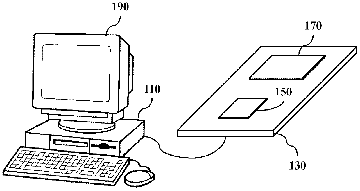
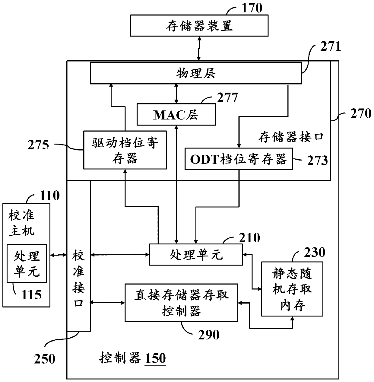
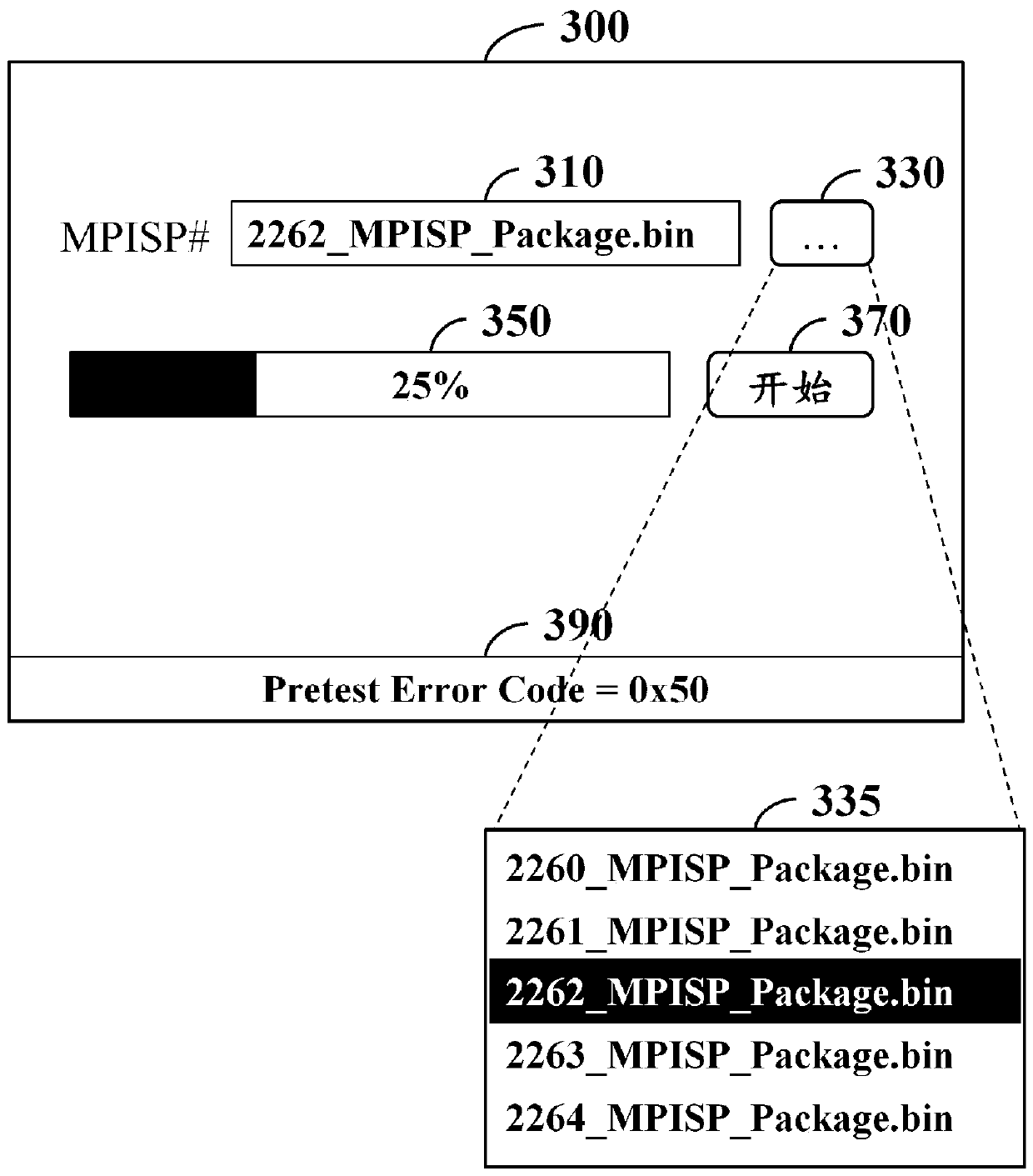
[0045] Embodiments of the present invention will be described below in conjunction with related drawings. In these drawings, the same reference numerals represent the same or similar components or method flows.

[0046] It must be understood that words such as "comprising" and "comprising" used in this specification are used to indicate the existence of specific technical features, values, method steps, job processing, components and / or components, but do not exclude possible Plus more technical features, values, method steps, job processes, components, components, or any combination of the above.

[0047] Words such as "first", "second", and "third" used in the present invention are used to modify the components in the claims, and are not used to indicate that there is a priority order, a prior relationship, or a component is prior relative to another component, or the chronological order in which method steps are performed, is only used to distinguish components with the sa...


PUM


Abstract

The invention provides an impedance configuration method of a memory interface, which is executed by a processing unit and comprises the following steps of: setting a first resistance value of an in-chip termination resistor associated with a first receiver as a first default resistance value; setting a second resistance value of a driving variable resistor associated with a second transmitter asa second default resistance value; executing a test for a plurality of test combinations, each combination comprising a third resistance value associated with the driving variable resistor of the first transmitter and a fourth resistance value associated with the in-chip termination resistor of the second receiver; and storing the test result of each test combination to a specific position of thestatic random access memory, so that the calibration host can obtain the test result of each test combination from the static random access memory and determine the impedance setting of the memory interface according to the test result.

Description

technical field [0001] The invention relates to a communication interface, in particular to an impedance configuration method of a memory interface and a computer-readable storage medium. Background technique [0002] After the speed of the DRAM (Dynamic Random Access Memory DRAM) bus reaches a high transfer rate, such as 500Mb / s or higher, system-level signaling problems may occur, for example, from connected peer devices (such as controllers, DRAM modules, etc.) lead lines produce reflections. The above-mentioned signal sending and receiving problems can be solved by calibrating the driver (Driver) and the on-chip termination resistor (On-Die Termination ODT). Therefore, the present invention proposes a method for configuring a memory interface and a computer-readable storage medium for calibrating the driver and the internal termination resistor in the memory interface. Contents of the invention [0003] In view of this, how to alleviate or eliminate the deficiencies ...

Claims


Application Information

Patent Timeline
Patent Type & Authority Applications(China)
IPC IPC(8): G11C29/50G11C29/56
CPCG06F11/2273G06F11/2221
Inventor 宋威良张启彬
Owner SILICON MOTION TECH CORP
Why Eureka
Try Eureka