Light emitting diode and driving method thereof, light source device and electronic equipment

A technology of light-emitting diodes and light-emitting layers, applied in circuits, electrical components, semiconductor devices, etc., can solve the problems of large spectral half-height width and low color purity of color light.

Active Publication Date: 2020-08-28
BOE TECH GRP CO LTD +1
View PDF4 Cites 3 Cited by
  • Summary
  • Abstract
  • Description
  • Claims
  • Application Information

AI Technical Summary

Problems solved by technology

[0003] The invention provides a light-emitting diode and its driving method, a light source device and electronic equipment, so as to solve the problems of the existing light-emitting diodes with large spectral half-width and low color purity

Method used


Image

  • Light emitting diode and driving method thereof, light source device and electronic equipment
  • Light emitting diode and driving method thereof, light source device and electronic equipment
  • Light emitting diode and driving method thereof, light source device and electronic equipment

Examples


Embodiment 1

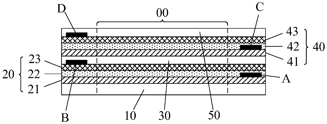
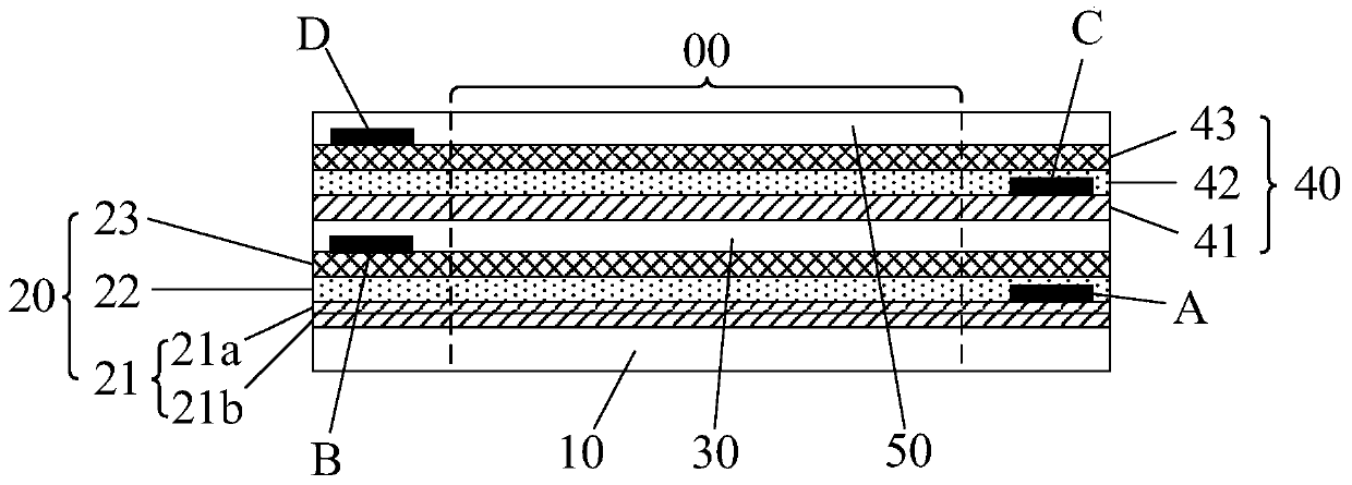
[0056] figure 1 A schematic cross-sectional view of a light-emitting diode according to Embodiment 1 of the present invention is shown, referring to figure 1 , the LED consists of:

[0057] Substrate 10;

[0058] A reflective luminescent layer 20, disposed on the substrate 10;

[0059] The first electrode A, the second electrode B and the first insulating layer 30 are separately arranged on the reflective light-emitting layer 20;

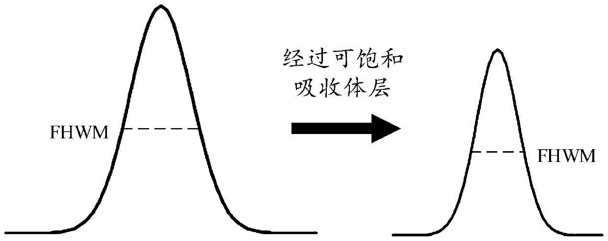
[0060] a saturable absorber layer 40, disposed on the first insulating layer 30;

[0061]The third electrode C, the fourth electrode D and the reflective composite layer 50 are separately arranged on the saturable absorber layer 40, and the reflectivity of the reflective luminescent layer 20 is greater than the reflectivity of the reflective composite layer 50;

[0062] Wherein, the orthographic projections of the saturable absorber layer 40 , the third electrode C, the fourth electrode D and the reflective composite layer 50 on the reflective l...

Embodiment 2

[0112] The embodiment of the present invention also discloses a driving method, which can be used to drive the above-mentioned light-emitting diodes, and the driving method includes:

[0113] The first positive voltage is input to the first electrode A, and the first negative voltage is input to the second electrode B.

[0114] Wherein, the first electrode A can be used as the anode for controlling the reflective luminescent layer 20, and the second electrode B can be used as the cathode for controlling the reflective luminescent layer 20, that is, in the embodiment of the present invention, the forward bias can be input to the reflective luminescent layer 20. pressure, thereby driving the reflective light-emitting layer 20 to emit light.

[0115] Optionally, the method also includes:

[0116] A second negative voltage is input to the third electrode C, and a second positive voltage is input to the fourth electrode D.

[0117] Wherein, the third electrode C can be used as th...

Embodiment 3

[0124] The embodiment of the present invention also discloses a light source device, including the above light emitting diode.

[0125] Wherein, in the field of display, the light source device may specifically be a backlight module, and the embodiment of the present invention does not specifically limit the light source device.

[0126] In an embodiment of the present invention, the light-emitting diode in the light source device includes a substrate, a reflective light-emitting layer disposed on the substrate, a first electrode, a second electrode, and a first insulating layer separately disposed on the reflective light-emitting layer, and are disposed on A saturable absorber layer on the first insulating layer, and a third electrode, a fourth electrode and a reflective composite layer separately arranged on the saturable absorber layer. Wherein, the reflectivity of the reflective luminescent layer is greater than that of the reflective composite layer, so as to ensure that ...


PUM


Abstract

The invention provides a light emitting diode and a driving method thereof, a light source device and electronic equipment, and relates to the technical field of semiconductors. The light emitting diode comprises a substrate, a reflective light emitting layer, a first electrode, a second electrode, a first insulating layer, a saturable absorber layer, a third electrode, a fourth electrode and a reflective composite layer, wherein the reflective light emitting layer disposed on the substrate; the first electrode, the second electrode and the first insulating layer are separately arranged on thereflective light emitting layer; the saturable absorber layer disposed on the first insulating layer; the third electrode, the fourth electrode and the reflective composite layer are separately arranged on the saturable absorber layer, and the reflectivity of the reflective light emitting layer is greater than that of the reflective composite layer; and orthographic projections of the saturable absorber layer, the third electrode, the fourth electrode and the reflective composite layer on the reflective light emitting layer are not overlapped with the first electrode and the second electroderespectively. According to the invention, after the light emitted by the reflective light emitting layer passes through the saturable absorber layer, the light with low energy is absorbed more, and the light with high energy is absorbed less, so that the full width at half maximum of the spectrum of the light emitting diode is reduced, and the color purity of the colored light of the light emitting diode is improved.

Description

technical field [0001] The invention relates to the technical field of semiconductors, in particular to a light emitting diode, a driving method thereof, a light source device and electronic equipment. Background technique [0002] A light emitting diode (Light Emitting Diode, LED) is a commonly used light-emitting device, which can release energy and emit light through the recombination of electrons and holes. It is widely used in many fields such as lighting, display, and medical treatment. Light-emitting diodes can efficiently convert electrical energy into light energy and have a wide range of uses in modern society. However, the spectral half-maximum width of the current light-emitting diode is large, so that the color purity of the light-emitting diode is relatively low. Contents of the invention [0003] The invention provides a light-emitting diode, a driving method thereof, a light source device and electronic equipment, so as to solve the problems of the existin...

Claims


Application Information

Patent Timeline
Patent Type & Authority Applications(China)
IPC IPC(8): H01L33/02H01L33/04H01L33/06H01L33/10H01L33/36H01L33/44H01L33/46H01L33/00
CPCH01L33/04H01L33/06H01L33/10H01L33/46H01L33/02H01L33/36H01L33/44H01L33/0062G09G3/32H01L25/0756H01L33/38H01L33/382
Inventor 解潇刘洋陈华斌李兴亮高英强王琳琳王瑞瑞
Owner BOE TECH GRP CO LTD
Why Eureka
Try Eureka