Treatment method for oxide on surface of copper
A surface oxide and treatment method technology, applied in the field of electronic packaging, can solve the problems of high equipment cost, copper surface pollution, complex process, etc., and achieve the effect of high average area, low cost and low process requirements
- Summary
- Abstract
- Description
- Claims
- Application Information
AI Technical Summary
Problems solved by technology
Method used
Image

Examples
Embodiment 1
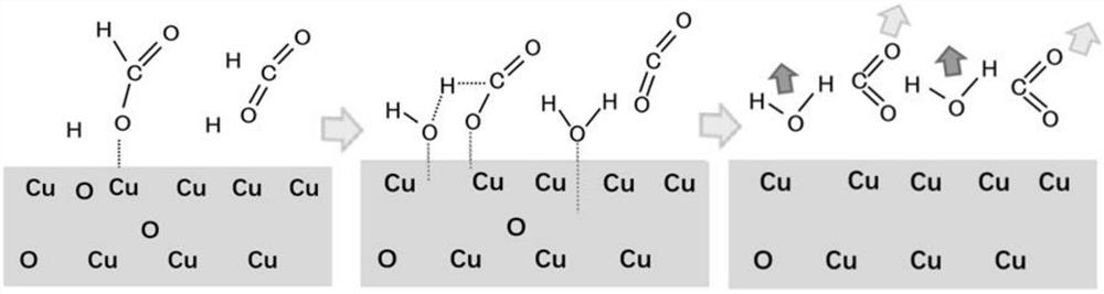
[0043] (1) Put the copper with oxides on the surface in the sealed cavity of the bonding equipment, vacuumize (below 10Pa), pass nitrogen gas for protection, and then heat to 200°C to obtain the copper to be processed.
[0044] (2) Feed into formic acid gas 30min continuously with the flow rate of 20mL / min, make described formic acid gas carry out reduction reaction after the copper surface to be treated that step (1) obtains is adsorbed, obtain the copper that removes surface oxide after desorption.
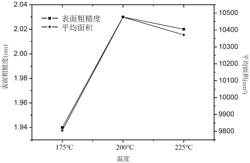
[0045] Carry out AFM test to the copper that removes surface oxide that the embodiment of the present invention 1 obtains, the result sees figure 2 shown. Depend on figure 2 It can be seen that the treatment method provided by Example 1 of the present invention has a good treatment effect, and the surface roughness of the copper surface obtained after treatment to remove surface oxides is 2.03nm, and the average area is 10455nm 2 ; and the copper surface is less polluted, and ...
Embodiment 2
[0047] (1) Place the copper with oxides on the surface in the sealed cavity of the bonding equipment, vacuumize (below 10Pa), pass nitrogen gas for protection, and then heat to 175°C to obtain the copper to be processed.
[0048] (2) Feed into formic acid gas 30min continuously with the flow rate of 20mL / min, make described formic acid gas carry out reduction reaction after the copper surface to be treated that step (1) obtains is adsorbed, obtain the copper that removes surface oxide after desorption.
[0049] Carry out AFM test to the copper that removes surface oxide that the embodiment of the present invention 2 obtains, the result sees figure 2 shown. Depend on figure 2 It can be seen that the treatment method provided by Example 2 of the present invention has a good treatment effect, and the surface roughness of the copper surface obtained after treatment to remove surface oxides is 1.94nm, and the average area is 9800nm 2 ; and the copper surface is less polluted, a...
Embodiment 3
[0051] (1) Put the copper with oxides on the surface in the sealed cavity of the bonding equipment, vacuumize (below 10Pa), pass nitrogen gas for protection, and then heat to 225°C to obtain the copper to be processed.
[0052] (2) Feed into formic acid gas 30min continuously with the flow rate of 20mL / min, make described formic acid gas carry out reduction reaction after the copper surface to be treated that step (1) obtains is adsorbed, obtain the copper that removes surface oxide after desorption.
[0053] Carry out AFM test to the copper that removes surface oxide that the embodiment of the present invention 3 obtains, the result sees figure 2 shown. Depend on figure 2 It can be seen that the treatment method provided by Example 3 of the present invention has a good treatment effect, and the surface roughness of the copper surface obtained after treatment to remove surface oxides is 2.02nm, and the average area is 10350nm 2 ; and the copper surface is less polluted, an...
PUM
| Property | Measurement | Unit |
|---|---|---|
| Surface roughness | aaaaa | aaaaa |
| Average area | aaaaa | aaaaa |
| Surface roughness | aaaaa | aaaaa |
Abstract
Description
Claims
Application Information
 - R&D Engineer
- R&D Manager
- IP Professional
- Industry Leading Data Capabilities
- Powerful AI technology
- Patent DNA Extraction
Browse by: Latest US Patents, China's latest patents, Technical Efficacy Thesaurus, Application Domain, Technology Topic.
© 2024 PatSnap. All rights reserved.Legal|Privacy policy|Modern Slavery Act Transparency Statement|Sitemap