3d NAND flash memory and its operation method
A flash memory and 3D technology, applied in the programming method of 3D NAND flash memory and the field of 3D NAND flash memory, can solve the problem of increasing writing time
- Summary
- Abstract
- Description
- Claims
- Application Information
AI Technical Summary
Problems solved by technology
Method used
Image
Examples
Embodiment Construction
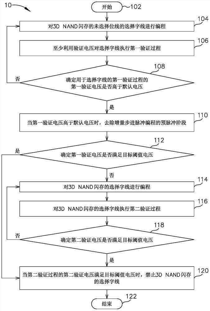
[0012] The pre-pulse phase is included in Incremental Stepped Pulse Programming (ISPP) of three-dimensional (3D) NAND flash memory. The pre-pulse phase of ISPP turns on the unselected upper select gate to reduce the channel potential difference, which increases the writing time of 3D NAND flash memory.
[0013] In order to reduce the writing time of 3D NAND flash memory, figure 1 is a schematic diagram of a programming process 10 for 3D NAND flash memory according to an embodiment of the present invention. The 3D NAND flash memory may include a plurality of bit lines, wherein the bit lines include a plurality of word line (WL) layers. The programming process 10 for 3D NAND flash includes the following steps:
[0014] Step 102: start.
[0015] Step 104: Program the selected word lines of the unselected bit lines of the 3D NAND flash memory.
[0016] Step 106: Perform a first verification process on the selected word line using at least a verification voltage.
[0017] Step...
PUM
 Abstract
Description
Claims
Application Information
 - R&D
- Intellectual Property
- Life Sciences
- Materials
- Tech Scout
- Unparalleled Data Quality
- Higher Quality Content
- 60% Fewer Hallucinations
Browse by: Latest US Patents, China's latest patents, Technical Efficacy Thesaurus, Application Domain, Technology Topic, Popular Technical Reports.
© 2025 PatSnap. All rights reserved.Legal|Privacy policy|Modern Slavery Act Transparency Statement|Sitemap|About US| Contact US: help@patsnap.com


