Photoelectric device, preparation method thereof and photoelectric detector

A photodetector, photoelectric device technology, applied in electrical components, semiconductor devices, circuits, etc., can solve the problems affecting the detection accuracy of photodetector efficiency, affecting the light absorption efficiency of the photosensitive layer, and the reflectivity of the photosensitive layer, etc. Photodetection efficiency and reliability, the effect of increasing light absorption efficiency and increasing area

Active Publication Date: 2020-09-08
BOE TECH GRP CO LTD
View PDF5 Cites 4 Cited by
  • Summary
  • Abstract
  • Description
  • Claims
  • Application Information

AI Technical Summary

Problems solved by technology

At present, the photodetector includes a photosensitive layer, and the photosensitive layer is a complete planar structure, but the photosensitive layer of the planar structure will cause 30% light reflection
[0003] In summary, the reflectivity of the photosensitive layer in the prior art photodetector is high, which affects the light absorption efficiency of the photosensitive layer and affects the efficiency and detection accuracy of the photodetector.

Method used


Image

  • Photoelectric device, preparation method thereof and photoelectric detector
  • Photoelectric device, preparation method thereof and photoelectric detector
  • Photoelectric device, preparation method thereof and photoelectric detector

Examples


Embodiment Construction

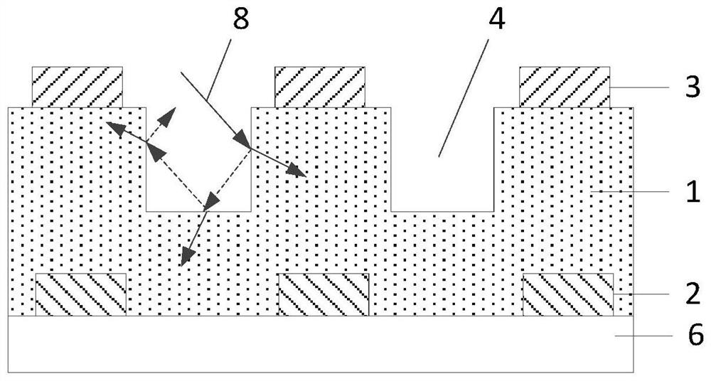
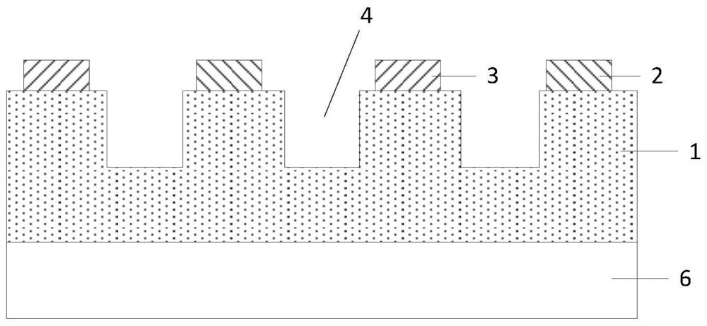
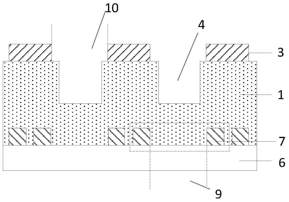
[0044] The embodiment of the present application provides an optoelectronic device, such as figure 1 As shown, the optoelectronic device includes: a photosensitive layer 1 located on a substrate 6, a first electrode 2 and a second electrode 3 respectively in contact with the photosensitive layer 1; In the area not covered by the second electrode 3 , the photosensitive layer 1 has a plurality of grooves 4 .

[0045] It should be noted that, if figure 1 As shown, the opening of the groove 4 faces the light-incident side of the photoelectric device. Even if the incident light 8 is reflected on the side wall of the groove 4, it can reach the bottom of the groove 4 again, and secondary reflection and refraction occur. Three times reflection and refraction can occur at the side walls of the groove 4 . That is, the light reflected for the first time will still reach other areas of the groove and be partially absorbed by the groove, and the incident light can be reflected and refrac...


PUM


Abstract

The invention discloses a photoelectric device, a preparation method thereof and a photoelectric detector to reduce the reflection of a photosensitive layer and improving the light absorption efficiency of the photosensitive layer. The embodiment of the invention provides the photoelectric device. The photoelectric device comprises a photosensitive layer located on a substrate, and a first electrode and a second electrode that make contact with the photosensitive layer respectively. And the photosensitive layer is provided with a plurality of grooves in an area which is not covered by the patterns of the first electrode and/or the second electrode.

Description

technical field [0001] The present application relates to the technical field of photoelectric devices, in particular to a photoelectric device, a preparation method thereof, and a photodetector. Background technique [0002] Photodetector technology has been extensively and intensively studied. At present, the photodetector includes a photosensitive layer, which is a complete planar structure, but the photosensitive layer of the planar structure will cause 30% light reflection. [0003] To sum up, the reflectivity of the photosensitive layer in the prior art photodetector is high, which affects the light absorption efficiency of the photosensitive layer and affects the efficiency and detection accuracy of the photodetector. Contents of the invention [0004] Embodiments of the present application provide a photoelectric device, a manufacturing method thereof, and a photodetector, which are used to reduce the reflection of the photosensitive layer and improve the light ab...

Claims


Application Information

Patent Timeline
Patent Type & Authority Applications(China)
IPC IPC(8): H01L31/0352H01L31/101H01L31/18
CPCH01L31/0352H01L31/101H01L31/18Y02P70/50
Inventor 李凡陈江博梁魁张硕孟凡理李达
Owner BOE TECH GRP CO LTD
Why Eureka
Try Eureka