Chip and patch packaging equipment

A patch packaging and chip technology, which is applied in the field of chip and patch packaging supporting equipment, can solve the problems of single polishing direction, reduce the protection strength of chips and patches, reduce the working efficiency and reliability of equipment, and achieve simple structure, The effect of improving machining accuracy and reliability

Inactive Publication Date: 2020-09-11
余颖
View PDF0 Cites 0 Cited by
  • Summary
  • Abstract
  • Description
  • Claims
  • Application Information

AI Technical Summary

Problems solved by technology

[0002] Before the chip and patch are packaged, it often involves the need to fully polish the burr of the chip and the patch. If the burr is not polished, the package will be punctured when the chip or patch is packaged and packaged, or it will be damaged during use. The existence of the above-mentioned burrs is not conducive to plastic packaging, etc., which will reduce the protection strength of chips and patches, and the existence of the above-mentioned burrs will reduce the yield rate of chips and patches in the manufacturing process, making the equipment inconvenient for efficient work and manufacturing Qualified chips and SMT products, the traditional way of grinding chips and SMTs is too single, and most of them use grinding sheets for grinding. When the patch is polished, it needs to be polished in all directions, but the grinding direction in the existing equipment is too single to achieve all-round grinding, which greatly reduces the working efficiency and reliability of the equipment

Method used


Image

  • Chip and patch packaging equipment
  • Chip and patch packaging equipment
  • Chip and patch packaging equipment

Examples


Embodiment Construction

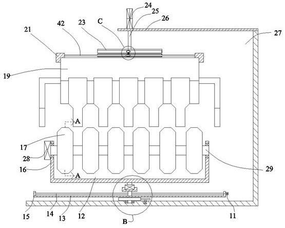
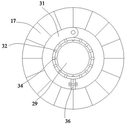
[0025] Such as Figure 1-Figure 4 As shown, the present invention is described in detail. For the convenience of description, the orientations mentioned below are now stipulated as follows: figure 1 The up, down, left, right, front and back directions of the projection relationship itself are consistent. A chip and patch packaging device of the present invention includes a support frame 26, and a penetrating inner cavity 27 is arranged in the supporting frame 26. There is an electronic device 19, a top clamping device capable of fully clamping the electronic device 19 is provided between the electronic device 19 and the upper side of the support frame 26, and the lower side of the penetrating inner cavity 27 is provided with A deburring device for deburring the electronic device 19 .

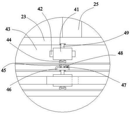
[0026] Beneficially, wherein, the top clamping device includes a lifting cylinder 24 fixed on the upper end surface of the support frame 26, and the lower side of the lifting cylinder 24 is con...


PUM


Abstract

The invention discloses chip and patch packaging equipment. The equipment comprises a supporting stand; a penetrative inner cavity is formed in the supporting stand; an electronic device is arranged inside the penetrating inner cavity; a top packaging and clamping device is arranged between the electronic device and the upper side of the supporting stand and can realize sufficient packaging and clamping of the electronic device; and a burr grinding device is arranged at the lower side of the penetrating inner cavity and is for burr grinding of the electronic device. The equipment is simple instructure; the equipment adopts a manner which can realize high-efficiency clamping of multiple sizes of chips and patches; high-efficiency burr grinding of the chips and the patches can be conductedin a multi-angle mode; and processing precision and reliability of the equipment are improved.

Description

technical field [0001] The invention relates to the technical field of supporting equipment for chip and chip packaging, in particular to chip and chip packaging equipment. Background technique [0002] Before the chip and patch are packaged, it often involves the need to fully polish the burr of the chip and the patch. If the burr is not polished, the package will be punctured when the chip or patch is packaged and packaged, or it will be damaged during use. The existence of the above-mentioned burrs is not conducive to plastic packaging, etc., which will reduce the protection strength of chips and patches, and the existence of the above-mentioned burrs will reduce the yield rate of chips and patches in the manufacturing process, making the equipment inconvenient for efficient work and manufacturing Qualified chips and SMT products, the traditional way of grinding chips and SMTs is too single, and most of them use grinding sheets for grinding. When the patch is polished, i...

Claims


Application Information

Patent Timeline
Patent Type & Authority Applications(China)
IPC IPC(8): B24B9/00B24B9/06B24B41/06B24B41/02B24B47/06B65B63/00H01L21/67
CPCB24B9/00B24B9/06B24B41/02B24B41/06B24B47/06B65B63/00H01L21/67092
Inventor 余颖
Owner 余颖
Why Eureka
Try Eureka