Chip-on-film (COF) package structure

A technology of film-on-chip packaging and packaging colloid, which is applied in the direction of electrical components, electrical solid devices, circuits, etc., can solve the problems of arching and gaps, poor heat dissipation efficiency, and the inability to effectively confirm that the heat dissipation patch is closely attached to the chip and packaging colloid Combination and other issues to achieve good cooling efficiency

Active Publication Date: 2020-09-15
CHIPMOS TECH INC
View PDF5 Cites 0 Cited by
  • Summary
  • Abstract
  • Description
  • Claims
  • Application Information

AI Technical Summary

Problems solved by technology

Generally speaking, the heat dissipation patch is attached to the chip packaging structure by rolling. Since the chip has a certain height and the underfill material (i.e., the encapsulant) covering the chip is in an irregular slope shape, the rolling When attaching the heat dissipation patch on the chip, there may be arches and gaps due to the heat dissipation patch not conforming to the tight fit between the chip

Method used


Image

  • Chip-on-film (COF) package structure
  • Chip-on-film (COF) package structure
  • Chip-on-film (COF) package structure

Examples


Embodiment Construction

[0042] The present invention will be described more fully with reference to the accompanying drawings of this embodiment. However, the present invention can also be embodied in various forms and should not be limited to the embodiments described herein. The thickness, size or size of layers or regions in the drawings may be exaggerated for clarity. The same or similar reference numerals denote the same or similar elements, and the following paragraphs will not repeat them one by one.

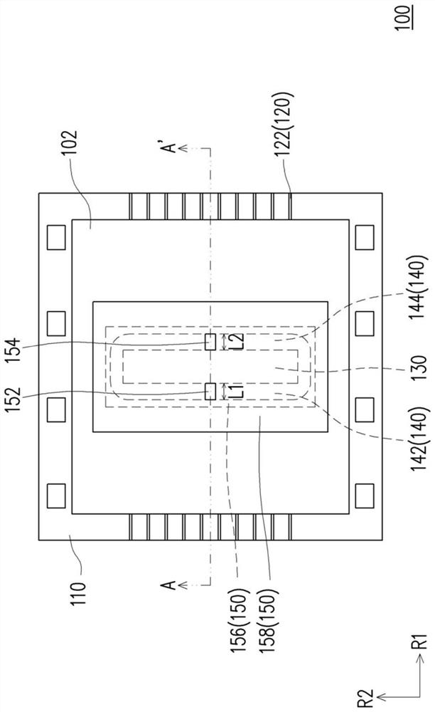
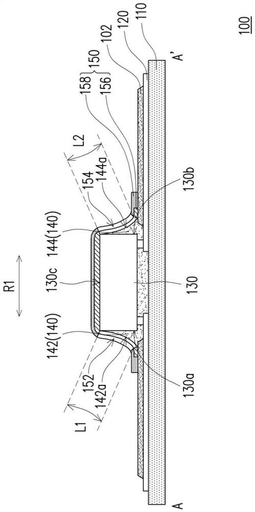
[0043] Figure 1A is a schematic top view of a chip-on-film packaging structure according to an embodiment of the present invention. Figure 1B yes Figure 1A Schematic cross-sectional view along section line A-A'. Please also refer to Figure 1A and Figure 1B , in this embodiment, the thin film chip-on-chip packaging structure 100 includes a flexible substrate 110 , a wiring layer 120 , a chip 130 , an encapsulant 140 and a heat dissipation patch 150 . The material of the flexible substrat...


PUM


Abstract

The invention provides a COF packaging structure including a flexible substrate, a circuit layer, a chip, an encapsulant and a heat sink. The circuit layer and the chip are located on the flexible substrate. The chip is electrically connected to the circuit layer. The circuit layer is located between the flexible substrate and the chip. The chip has a first side surface and a second side surface opposite to each other. The encapsulant fills at least a gap between the flexible substrate and the chip. The encapsulant includes a first part covering the first side surface of the chip and a secondpart covering the second side surface of the chip. The heat sink is located on the flexible substrate and covers the chip and the encapsulant. The heat sink has at least two openings, and the two openings are respectively located on opposite sides of the chip. One of the two openings partially exposes the first part of the encapsulant, and the other of the two openings partially exposes the secondpart of the encapsulant.

Description

technical field [0001] The invention relates to a package structure, in particular to a film-on-chip package structure. Background technique [0002] In order to improve the heat dissipation effect of the current Chip on Film package (COF), heat dissipation patches are attached on the surface of the package structure, especially on the surface with the chip. Generally speaking, the heat dissipation patch is attached to the chip packaging structure by rolling. Since the chip has a certain height and the underfill material (i.e., the encapsulant) covering the chip is in an irregular slope shape, the rolling When attaching the heat dissipation patch on the chip in this way, there may be arches and gaps due to the heat dissipation patch not conforming to the tight fit of the chip and the encapsulant. In addition, since the heat dissipation patch will completely cover the chip and the encapsulation compound, it is impossible to effectively confirm whether the heat dissipation pa...

Claims


Application Information

Patent Timeline
IPC IPC(8): H01L23/367
CPCH01L23/3672H01L2224/32225H01L2224/73204H01L2224/16225H01L2924/00
Inventor 陈崇龙
Owner CHIPMOS TECH INC
Why Eureka
Try Eureka