Semiconductor packaging body and manufacturing method thereof

A manufacturing method and semiconductor technology, applied in semiconductor/solid-state device manufacturing, semiconductor devices, semiconductor/solid-state device components, etc., can solve the problems of wafer-level chip-scale package warpage, thick packaging colloid, and unfavorable wafer-level Chip size package miniaturization and other issues to achieve the effect of good heat dissipation efficiency

Inactive Publication Date: 2016-11-23
POWERTECH TECHNOLOGY
View PDF3 Cites 0 Cited by
  • Summary
  • Abstract
  • Description
  • Claims
  • Application Information

AI Technical Summary

Problems solved by technology

Generally speaking, the thickness of the encapsulant formed by the compression molding process is relatively thick, which is not conducive to the miniaturization of the wafer-level chip size package.
In addition, due to the low thermal conductivity and poor heat dissipation effect of the encapsulant, most of the heat generate

Method used


Image

  • Semiconductor packaging body and manufacturing method thereof
  • Semiconductor packaging body and manufacturing method thereof
  • Semiconductor packaging body and manufacturing method thereof

Examples


Embodiment Construction

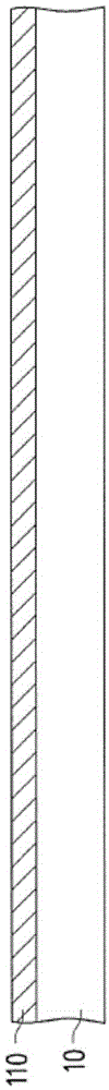
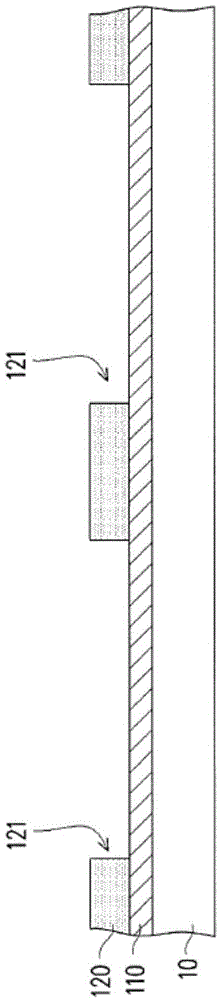
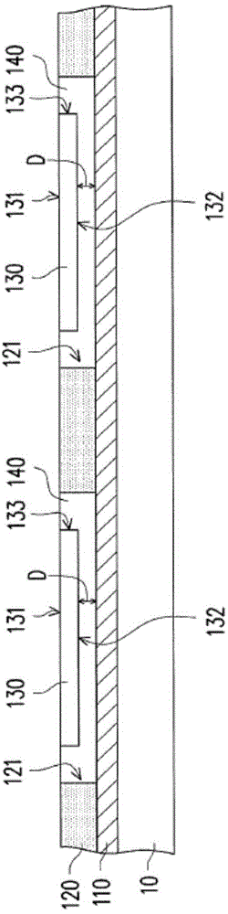
[0045] Figure 1A to Figure 1G A manufacturing flow of a semiconductor package according to an embodiment of the present invention is shown. Please refer to Figure 1A Firstly, the carrier 10 is provided, and the heat dissipation material layer 110 is formed on the carrier 10 . For example, the carrier 10 can be a plate made of hard material or flexible material, or a release film (such as a thermal release adhesive film, an ultraviolet light release adhesive film or other suitable adhesive films), but the present invention is for The material of the carrier 10 is not limited in any way. Here, the heat dissipation material layer 110 is temporarily fixed on the carrier 10 by, for example, gluing, so as to facilitate subsequent manufacturing processes. In this embodiment, the heat dissipation material layer 110 may be made of aluminum, magnesium, copper, silver, gold or other metals or metal alloys with good thermal conductivity, or graphite or other non-metallic materials wit...


PUM


Abstract

The invention provides a semiconductor packaging body and a manufacturing method thereof. The semiconductor packaging body comprises an insulating layer, a chip, a thermal interface material, a heat radiation cover body and a reconfiguration line layer, and is characterized in that the insulating layer is provided with an accommodating opening; the chip is arranged in the accommodating opening; the chip is provided with an active surface, a back surface opposite to the active surface, and a side surface connecting the active surface and the back surface; the thermal interface material fills the accommodating opening so as to at least coat the side surface of the chip and exposes the active surface; the reconfiguration line layer and the heat radiation cover body are respectively configured at two sides of the insulating layer; the heat radiation cover body is thermally coupled to the chip through the thermal interface material; and the reconfiguration line layer covers the active surface of the chip and the thermal interface material, and the reconfiguration line layer is electrically connected with the chip. The semiconductor packaging body provided by the invention has excellent heat radiation efficiency.

Description

technical field [0001] The present invention relates to a packaging body and its manufacturing method, and in particular to a semiconductor packaging body and its manufacturing method. Background technique [0002] In order to meet the requirements of light, thin and small electronic products, semiconductor packages, which are the core components of electronic products, are also developing in the direction of miniaturization. In recent years, the industry has developed a chip-scale package (Chip Scale Package, CSP for short) miniaturized semiconductor package, which is characterized in that the size of the aforementioned chip-scale package is approximately equal to the size of its chip or slightly larger than the size of its chip. size. On the other hand, in addition to miniaturization in size, the semiconductor package also needs to improve the integration (integrity) and the input / output terminals (Input / Output, referred to as I / O) for electrical connection with external ...

Claims


Application Information

Patent Timeline
IPC IPC(8): H01L23/367H01L23/31H01L21/48H01L21/56
CPCH01L21/568H01L2224/04105H01L2224/12105H01L2224/19H01L2224/32225H01L2224/32245H01L2224/73267H01L2224/92244H01L2224/97
Inventor 徐守谦藤岛浩幸
Owner POWERTECH TECHNOLOGY
Why Eureka
Try Eureka