Mounting devices for semiconductor packages

A mounting device and semiconductor technology, applied in the direction of semiconductor devices, semiconductor/solid-state device components, electric solid-state devices, etc., can solve problems such as channels that hinder semiconductor packaging temperature monitoring, improve clearance and creepage distance, reduce assembly and The effect of material cost

Active Publication Date: 2020-09-15
MAHLE INT GMBH
View PDF5 Cites 0 Cited by
  • Summary
  • Abstract
  • Description
  • Claims
  • Application Information

AI Technical Summary

Problems solved by technology

In this regard, conventional mounting devices such as steel clips are simple mechanical devices that block access to temperature monitoring in semiconductor packages

Method used


Image

  • Mounting devices for semiconductor packages
  • Mounting devices for semiconductor packages
  • Mounting devices for semiconductor packages

Examples


Embodiment Construction

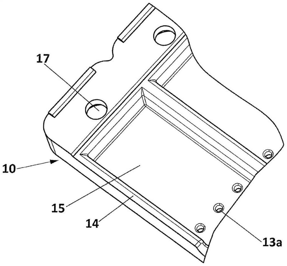
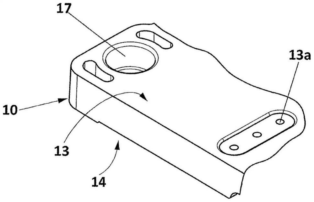
[0021] Figure 1A Shown is a bottom view of an example of a mounting device (10) for a heat generating semiconductor package, the mounting device (10) comprising a bottom side (14) having one or more cavities (15), each with a To accommodate a semiconductor package not shown in the figure. Examples of semiconductor packages are eg TO220 packages and TO247 packages. Mounting device (10) includes Figure 1B Top side (13) shown. The top side (13) includes a plurality of holes (13a) for allowing contact pins (12) of the semiconductor package (11) to extend from the bottom side (14) of the device to the top side (13). Furthermore, the mounting device (10) comprises a fixing device comprising screw holes (17) suitable for receiving fixing screws for fixing the mounting device (10) with the semiconductor package to the heat dissipation structure.

[0022] In some examples, the heat dissipation structure may be a heat sink or a cold plate or part chassis.

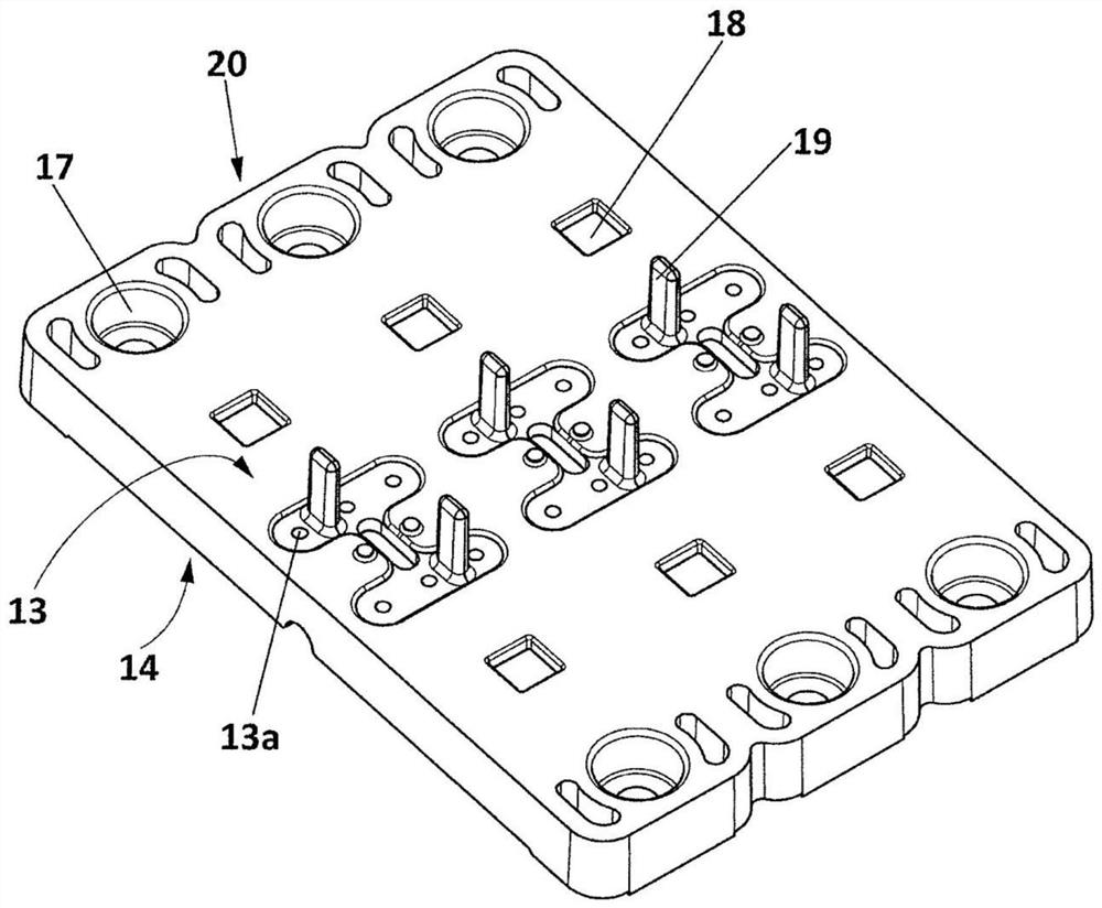
[0023] Figure 2A A t...


PUM


Abstract

Mounting device (10) for semiconductor packages (11), the device (10) comprising a bottom side (14) comprising one or more cavities (15) to house semiconductor packages (11); a top side (13) comprising a plurality of holes (13a) extending from the bottom side (14) to the top side (13) for accommodating contact pins (12) of the semiconductor package (11); and fixation means to fix the device (10) housing the semiconductor packages (11) to a heat dissipation structure.

Description

technical field [0001] The present invention relates to mounting devices for semiconductor packages. Background technique [0002] Semiconductor packages are commonly used in electronic circuit applications. When conduction cooling is required, a common semiconductor device packaging arrangement includes a substrate that acts as a heat sink and an enclosure that can be placed over the substrate to form an internal cavity above the substrate. Integrated circuits, such as semiconductor chips, and other electronic components may be placed within the cavity and electrically connected to conductive leads / contact pins protruding from the housing. Conductive leads enable electrical connection between the package and a socket, such as a printed circuit board (PCB). Thus, the packaged arrangement allows easy electrical connection between the circuit and external devices, while protecting the semiconductor chip and electrical connections from environmental conditions such as moistur...

Claims


Application Information

Patent Timeline
Patent Type & Authority Applications(China)
IPC IPC(8): H01L23/40H01L23/367
CPCH01L23/3672H01L23/3675H01L23/40H01L23/4006H01L25/115H05K7/20472H05K7/2049H05K3/301H01L23/34H01L2023/4031H01L2023/4062H01L2023/4087H05K2201/10H05K2201/10598
Inventor 弗朗西斯科·冈萨雷斯·埃斯潘托比约恩·哈尔伯格约瑟·安东尼奥·卡斯蒂略
Owner MAHLE INT GMBH
Why Eureka
Try Eureka