Mask plate and method for exposing wafer with protrusions

A technology of mask plate and convex part, which is applied in the field of mask plate for wafer exposure with convex part, can solve the problems of expensive price, resolution not meeting the process requirements, wafer alignment and other problems, and achieve saving Cost, High Resolution Requirements, Effects of Improving Alignment Accuracy

Pending Publication Date: 2020-09-29
SIEN QINGDAO INTEGRATED CIRCUITS CO LTD
View PDF4 Cites 2 Cited by
  • Summary
  • Abstract
  • Description
  • Claims
  • Application Information

AI Technical Summary

Problems solved by technology

[0003] However, since the edge of the back side of the wafer processed by the Taiko process (referred to as Taiko wafer) remains, there will be a ring-shaped raised part (Taiko ring) 285-335 μm higher than the exposure surface. The engraving machine cannot directly align the wafer with the convex part, and it is expensive to develop and modify, and there is also the risk of the lens hitting the ring-shaped convex, while the mask aligner (MaskAligner ) Although the back alignment of the Taiko wafer can be realized by infrared light, the existence of the ring-shaped raised portion prevents the mask plate from approaching the alignment marks on the back of the Taiko wafer, so the resolution still cannot reach the process Require
[0004] In addition, the existing Taiko wafer back exposure technology, when the gap between the mask plate and the center of the wafer is within the height range of the ring-shaped raised part, the resolution is about 30 μm, which cannot meet the requirements of the IGBT back implant photo. layer (IGBTbackside implant photo layer) process requires a high resolution of 2μm, so it is urgent to provide a mask and method for wafer exposure with bumps to meet the high resolution requirements of the Taiko wafer backside. exposure needs

Method used


Image

  • Mask plate and method for exposing wafer with protrusions
  • Mask plate and method for exposing wafer with protrusions
  • Mask plate and method for exposing wafer with protrusions

Examples


Embodiment 1

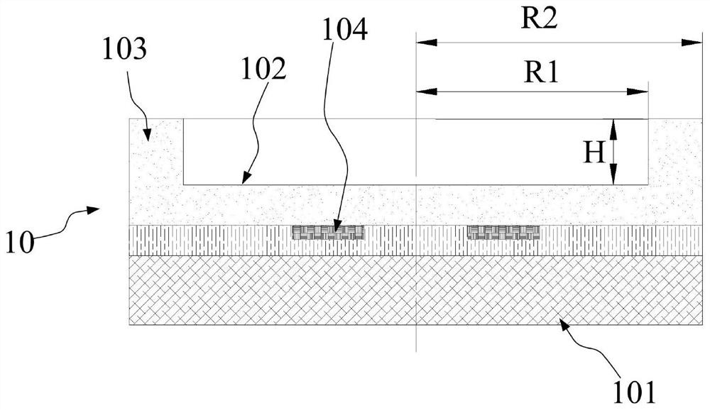
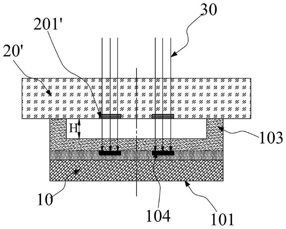
[0052] This embodiment provides a Figure 4-5Reticles for exposure of bumped wafers are shown, which are used as Figure 6-7 Exposure of a wafer 10 with a raised portion on the exposure surface shown in , the side of the wafer 10 facing the mask 20 is provided with a plurality of raised portions 103 (can also be one), the mask A graphic layer (not shown) and an alignment mark 104 are arranged on the mask plate 20, and a hole capable of receiving the protrusion 103 is provided on the side of the mask plate 20 facing the wafer 10. Notch 202.

[0053] Such as Figure 8 As shown, before exposure, insert all the protrusions 103 of the wafer 10 into the corresponding notches 202 of the mask 20, and adjust the insertion of the protrusions 103 to the corresponding positions according to the required resolution. After the depth in the above-mentioned notch 202 is reached so that the predetermined exposure gap requirement is reached between the mask plate 20 and the exposure surface ...

Embodiment 2

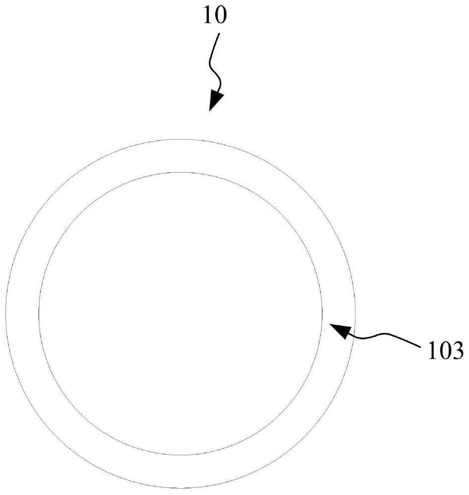
[0058] This embodiment provides a Figure 9-10 The mask plate 20 shown for wafer exposure with bumps can also realize the Figure 6-7 In the high-resolution exposure of the wafer 10 shown, the difference between the mask plate in this embodiment and the mask plate in Embodiment 1 is that the notch 202 of the mask plate 20 in this embodiment is an annular groove 2021. A plurality of protrusions 103 that are discretely distributed around the circumference are all inserted into the annular groove 2021 .

Embodiment 3

[0060] This embodiment provides a Figure 12-13 The mask plate 20 shown for wafer exposure with bumps can also realize the Figure 6-7 In the high-resolution exposure of the wafer 10 shown, the difference between the mask plate in this embodiment and the mask plate in Embodiment 1 is that the mask plate 20 in this embodiment is provided with a plurality of Figure 6-7 In the independent notch 202 corresponding to the plurality of raised parts 103, the plurality of raised parts 103 distributed in a discrete shape during exposure are respectively inserted into the corresponding notch 202 to reduce the distance between the mask plate 20 and the exposure surface. exposure gap.


PUM


Abstract

The invention provides a mask plate and method for exposing a wafer with protrusions. At least one protrusion is arranged on the side, facing the mask plate, of the wafer, a graphic layer and alignment marks are arranged on the mask plate, and notches capable of allowing the protrusions to be inserted therein are further formed in the side, facing the wafer, of the mask plate. Before the method isused for exposure, all the protrusions of the wafer are inserted into the notches corresponding to the mask plate, and the depth of the protrusions inserted into the notches is adjusted according tothe required resolution so as to keep the positions of the mask plate and the wafer unchanged after a preset exposure gap requirement is met between the mask plate and the exposure surface of the wafer, and exposing is carried out on the wafer by using an exposure light source. By utilizing the mask plate and the exposure method, a preset gap can be formed between the mask plate and the wafer exposure surface without improving a stepping photoetching machine, so that the alignment precision and the resolution ratio are improved, and the cost is saved.

Description

technical field [0001] The invention relates to the technical field of integrated circuits, in particular to the field of photolithography, and more specifically to a mask plate and a method for exposing wafers with raised portions. Background technique [0002] The grinding process on the back of the wafer in the prior art mainly includes the Taiko process and the traditional non-Taiko (non-Taiko) grinding process. When the wafer is ground by the Taiko process, the outer edge of the wafer will be kept, and only the inside of the wafer will be ground and thinned. This process can reduce the handling risk of thin wafers, and can reduce the warpage of wafers caused by traditional grinding processes, and improve the strength of wafers. [0003] However, since the edge of the back side of the wafer processed by the Taiko process (referred to as Taiko wafer) remains, there will be a ring-shaped raised part (Taiko ring) 285-335 μm higher than the exposure surface. The engraving ...

Claims


Application Information

Patent Timeline
Patent Type & Authority Applications(China)
IPC IPC(8): G03F1/38G03F1/42
CPCG03F1/38G03F1/42
Inventor 郭素华
Owner SIEN QINGDAO INTEGRATED CIRCUITS CO LTD
Why Eureka
Try Eureka