Check patentability & draft patents in minutes with Patsnap Eureka AI!

JTAG debugging circuit and computer debugging tool

A technology for debugging circuits and debugging tools, applied in computing, electrical digital data processing, instruments, etc., can solve the problems of complex JTAG link design and rising cost, and achieve the effect of improving design efficiency and reducing product defect rate

Inactive Publication Date: 2020-09-29
INSPUR SUZHOU INTELLIGENT TECH CO LTD
View PDF0 Cites 0 Cited by
  • Summary
  • Abstract
  • Description
  • Claims
  • Application Information

AI Technical Summary

Problems solved by technology

The JTAG link design based on debugging is complicated, and multiple logic chips are used for switching, which brings additional cost increase

Method used


Image

  • JTAG debugging circuit and computer debugging tool

Examples


Embodiment Construction

[0020] In order to make the object, technical solution and advantages of the present invention clearer, the embodiments of the present invention will be further described in detail below in conjunction with specific embodiments and with reference to the accompanying drawings.

[0021] It should be noted that all expressions using "first" and "second" in the embodiments of the present invention are to distinguish two entities with the same name but different parameters or parameters that are not the same, see "first" and "second" It is only for the convenience of expression, and should not be construed as a limitation on the embodiments of the present invention, which will not be described one by one in the subsequent embodiments.

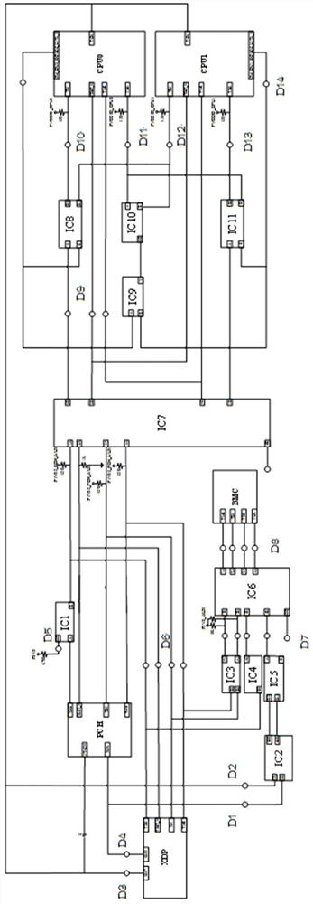
[0022] Based on the above purpose, the first aspect of the embodiments of the present invention proposes a JTAG debugging circuit. figure 1 What is shown is a schematic diagram of an embodiment of the JTAG debugging circuit provided by the present i...


PUM


Abstract

The invention discloses a JTAG debugging circuit and a computer debugging tool. The JTAG debugging circuit comprises the following parts: an XDP of which a first clock output interface is connected toa clock receiving interface of a PCH, a second clock output interface is connected to a clock receiving interface of a CPU and a data transmission interface is respectively connected to a data transmission interface of the PCH and a data transmission interface of the CPU, a BMC conversion chip of which a first clock output interface is connected to the clock receiving interface of the PCH, a second clock output interface is connected to the clock receiving interface of the CPU and a data transmission interface is connected to the data transmission interface of the PCH and the data transmission interface of the CPU, and a BMC of which a first clock output interface is connected to a clock receiving interface of the BMC conversion chip and a data transmission interface is connected to a data receiving interface of the BMC conversion chip. According to the invention, integration of multiple debugging modes can be realized, the design efficiency can be greatly improved, and the reject ratio of products is reduced.

Description

technical field [0001] The invention relates to the technical field of computer debugging, in particular to a JTAG debugging circuit and a computer debugging tool. Background technique [0002] JTAG (Joint Test Action Group, Joint Test Working Group) is an international standard test protocol (IEEE 1149.1 compatible), mainly used for chip internal testing. Now most advanced devices support JTAG protocol, such as CPU, PCH, BMC, CPLD devices and so on. The standard JTAG interface is 4 lines: TMS, TCK, TDI, TDO, which are mode selection, clock, data input and data output lines respectively. [0003] JTAG was originally used to test the chip. The basic principle of JTAG is to define a TAP (Test Access Port) inside the device, and test the internal nodes through a dedicated JTAG test tool. The JTAG test allows multiple devices to be connected in series through the JTAG interface to form a JTAG chain, which can test each device separately. [0004] In server design, JTAG is als...

Claims


Application Information

Patent Timeline
Patent Type & Authority Applications(China)
IPC IPC(8): G06F11/267G06F11/273
CPCG06F11/267G06F11/273
Inventor 张敏王鹏杨德晓付水论叶明洋
Owner INSPUR SUZHOU INTELLIGENT TECH CO LTD
Features
  • R&D
  • Intellectual Property
  • Life Sciences
  • Materials
  • Tech Scout
  • Unparalleled Data Quality
  • Higher Quality Content
  • 60% Fewer Hallucinations
Learn More