Method and device for optimizing technological process, storage medium and semiconductor processing equipment

A technology of process flow and process steps, applied in the field of semiconductor processing equipment, computer-readable storage medium, and devices for optimizing process flow, can solve problems such as affecting the process, timeliness, and poor operability, and achieve strong timeliness and operability. The effect of improving and increasing productivity

Pending Publication Date: 2020-09-29
BEIJING NAURA MICROELECTRONICS EQUIP CO LTD
View PDF14 Cites 0 Cited by
  • Summary
  • Abstract
  • Description
  • Claims
  • Application Information

AI Technical Summary

Problems solved by technology

Apparently, in this related technology, user intervention is required when a glow failure occurs, and the timeliness and operability are poor. For some special processes, the process may even be affected due to long-term recovery

Method used


Image

  • Method and device for optimizing technological process, storage medium and semiconductor processing equipment
  • Method and device for optimizing technological process, storage medium and semiconductor processing equipment

Examples


Embodiment Construction

[0050] Specific embodiments of the present invention will be described in detail below in conjunction with the accompanying drawings. It should be understood that the specific embodiments described here are only used to illustrate and explain the present invention, and are not intended to limit the present invention.

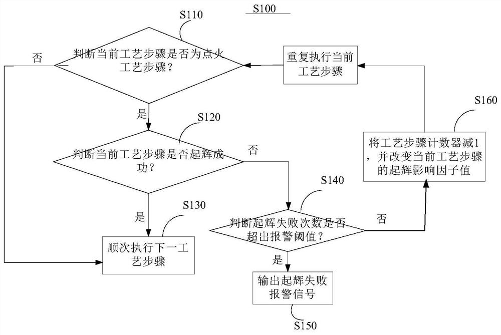
[0051] The first aspect of the present invention relates to a method for optimizing a process flow. The process flow includes several process steps performed in sequence. For example, in the magnetron sputtering process process, the process flow generally includes an air intake process step and an ignition process step. , deposition process step, cooling process step, finishing process step and other five process steps. Of course, this technological process can also be applied to other technological processes, and any technological process including an ignition process step in the technological process can be applied to the method for optimizing the technologica...


PUM


Abstract

The invention discloses a method and device for optimizing a technological process, a storage medium and semiconductor processing equipment. The method comprises the following steps: step S110, judging whether a current process step is an ignition process step or not, and if so, executing step S120; if not, executing the step S130; S120, judging whether the current process step is successfully started or not, and if so, executing the step S130; if not, executing the step S140; S130, executing the next process steps in sequence; step S140, judging whether the number of times of ignition failureexceeds an alarm threshold value or not, if so, executing step S150, and if not, executing the step S160; S150, outputting an ignition failure alarm signal; and step S160, subtracting 1 from a process step counter, changing an ignition influence factor value of the current process step, repeatedly executing the current process step and returning to the step S110. When an accidental ignition failure phenomenon exists, a user does not need to intervene, so that the timeliness of the process flow is relatively strong, the operability is improved, the process flow can be normally carried out, andthe productivity is improved.

Description

technical field [0001] The invention relates to the technical field of semiconductor manufacturing, in particular to a method for optimizing a process flow, a device for optimizing a process flow, a computer-readable storage medium, and a semiconductor processing device. Background technique [0002] Physical vapor deposition (Physical Vapor Deposition, PVD) refers to the use of low-voltage, high-current arc discharge technology under vacuum conditions to evaporate the target material by gas discharge, and to cause ionization and ignition of the evaporated material and gas. Under the accelerated action of the vaporized substance and its reaction product, it will be deposited on the workpiece (usually a wafer). This technology has been widely used in integrated circuit (Integrated Circuit, IC), light-emitting diode (Light-emitting Diode, LED), photovoltaic, flat panel display and other fields. [0003] Occasional ignition failures may occur due to abnormal hardware or unstab...

Claims


Application Information

Patent Timeline
Patent Type & Authority Applications(China)
IPC IPC(8): H01L21/67
CPCH01L21/67276H01L21/67253
Inventor 金晨韩彬李建银
Owner BEIJING NAURA MICROELECTRONICS EQUIP CO LTD
Why Eureka
Try Eureka