
Wafer drying method and system

A wafer drying and wafer technology, applied in electrical components, semiconductor/solid-state device manufacturing, circuits, etc., can solve the problems of poor wafer drying effect, easy residual liquid, water marks, etc., to avoid water marks and improve the crystallinity. The effect of the round drying effect

Active Publication Date: 2020-10-02
华海清科(北京)科技有限公司
View PDF12 Cites 2 Cited by
  • Summary
  • Abstract
  • Description
  • Claims
  • Application Information

AI Technical Summary

Problems solved by technology

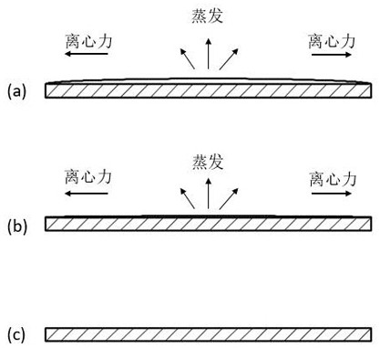
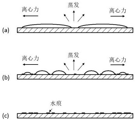
The traditional rotary drying method, because the thickness of the remaining water film after drying is very large, which can reach micron level and above, it is easy to cause water mark defects
[0004] To sum up, the prior art has the problem of poor wafer drying effect and easy residual liquid

Method used


Image

  • Wafer drying method and system
  • Wafer drying method and system
  • Wafer drying method and system

Examples


Embodiment Construction

[0040] The technical solutions of the present invention will be described in detail below in conjunction with specific embodiments and accompanying drawings. The examples described here are specific implementations of the present invention and are used to illustrate the concept of the present invention; these descriptions are all explanatory and exemplary, and should not be construed as limiting the implementation of the present invention and the protection scope of the present invention . In addition to the embodiments described here, those skilled in the art can also adopt other obvious technical solutions based on the claims of the application and the contents disclosed in the specification, and these technical solutions include adopting any modifications made to the embodiments described here. Obvious alternatives and modified technical solutions.

[0041] In order to illustrate the technical solutions of the present invention, specific examples are used below to illustra...


PUM

PropertyMeasurementUnit
contact angleaaaaaaaaaa

Abstract

The invention discloses a wafer drying method and system. The wafer drying method comprises the steps that a wafer is made to rotate around a center shaft perpendicular to the surface of the wafer; amixed liquid is supplied to the surface of the wafer to form a liquid film of the mixed liquid on the surface of the wafer, wherein the mixed liquid is formed by dissolving a certain concentration ofa surface active material into a cleaning liquid, and the surface tension of the mixed liquid is lower than the surface tension of water; and dry gas is sprayed to the surface of the wafer to generatea Marangoni effect to enable the liquid film to be stripped from the surface of the wafer so as to realize wafer drying. The wafer drying system comprises a rotating unit, a liquid supply unit and adrying unit.

Description

technical field [0001] The invention relates to the technical field of wafer post-processing, in particular to a wafer drying method and system. Background technique [0002] Wafer manufacturing is a key link that restricts the development of the ultra / very large scale integrated circuit (ie chip, IC, Integrated Circuit) industry. With the continuation of Moore's Law, the feature size of integrated circuits continues to shrink and approach the theoretical limit, and the requirements for wafer surface quality are becoming more and more stringent. Therefore, the control of defect size and quantity in the wafer manufacturing process is becoming more and more strict. In the logic chip manufacturing process, when the feature size is developed from 14nm to 7nm, the control range of pollutants above 19nm is also reduced from 100 to 50, gradually approaching the limits of cleaning technology and measurement technology. Contaminants are an important factor that causes wafer surface ...

Claims


Application Information

Patent Timeline
Patent Type & Authority Applications(China)
IPC IPC(8): H01L21/67
CPCH01L21/67034
Inventor 曹自立李长坤刘健赵德文
Owner 华海清科(北京)科技有限公司
Learn More