Display panel, preparation method thereof and display device

A technology for a display panel and a bending area, applied in the fields of its preparation, display device, and display panel, can solve the problems of difficult manufacturing process, complicated process, influence on display effect, etc., so as to avoid bending fracture, relieve stress, and reduce risk. Effect

Inactive Publication Date: 2020-10-13
WUHAN CHINA STAR OPTOELECTRONICS SEMICON DISPLAY TECH CO LTD
View PDF9 Cites 9 Cited by
  • Summary
  • Abstract
  • Description
  • Claims
  • Application Information

AI Technical Summary

Problems solved by technology

[0004] An embodiment of the present invention provides a display panel, which is used to solve the problem that the bendable display panel in the prior art cannot achieve high resolution, the process is complicated, the manufacturing process is difficult, and the electrical properties of the thin film transistor will change with the bend. Technical problems that drift and affect the display effect

Method used


Image

  • Display panel, preparation method thereof and display device
  • Display panel, preparation method thereof and display device
  • Display panel, preparation method thereof and display device

Examples


Embodiment Construction

[0020] The technical solutions in the embodiments of the present invention will be clearly and completely described below in conjunction with the accompanying drawings in the embodiments of the present invention. Obviously, the described embodiments are only a part of the embodiments of the present invention, rather than all the embodiments. Based on the embodiments of the present invention, all other embodiments obtained by those skilled in the art without creative work shall fall within the protection scope of the present invention.

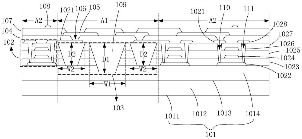
[0021] Such as figure 1 As shown, the schematic diagram of the basic structure of the display panel provided by the embodiment of the present invention, from which the various components of the present invention and the relative positional relationship between the components can be seen very intuitively. The display panel is divided into curved In the folding area A1 and the non-bending area A2, the display panel includes: a substrate layer 101; a ...


PUM


Abstract

The invention provides a display panel, a preparation method thereof and a display device. The display panel is divided into a bending area and a non-bending area. The display panel comprises a substrate layer, a thin film transistor layer which is located on the substrate layer and corresponds to the non-bending area, an organic filling layer which is located on the substrate layer and corresponds to the bending area, a planarization layer which is located on the thin film transistor layer and the organic filling layer, and a pixel electrode which is located on the planarization layer, wherein the pixel electrode in the bending area is connected with a source electrode of the thin film transistor layer in the non-bending area through a metal wire, the organic filling layer comprises a plurality of second via holes, and the plurality of second via holes are filled with organic photoresists. The plurality of via holes are formed below the metal wires in the bending area and are filled with the organic photoresists, so that the risk of breakage of the metal wires can be reduced, and the stress of each film layer during bending is greatly relieved.

Description

Technical field [0001] The present invention relates to the field of display technology, in particular to a display panel, a preparation method thereof and a display device. Background technique [0002] A rigid OLED display panel becomes a bendable flexible OLED display panel. The biggest challenge is the stress problem. Because the entire display screen is composed of multiple layers of materials, the material is squeezed during bending, which will easily break and affect the display. [0003] The prior art bendable OLED display panel uses the method of etching the inorganic film layer in the bending area and filling the organic photoresist to release the stress during bending. However, this structure has certain limitations, such as being unable to achieve High resolution, complex process, and difficult manufacturing process. In addition, because the entire thin film transistor is bent during bending, there is still a risk of wire breakage, and the electrical properties of the t...

Claims


Application Information

Patent Timeline
Patent Type & Authority Applications(China)
IPC IPC(8): G09F9/30H01L27/32H01L27/12
CPCG09F9/301H01L27/1214H10K59/12H10K59/124H10K77/111H10K59/131H10K59/00H10K59/122H10K2102/311H10K71/00H10K59/123H10K59/1201
Inventor 胡俊艳
Owner WUHAN CHINA STAR OPTOELECTRONICS SEMICON DISPLAY TECH CO LTD
Why Eureka
Try Eureka