OLED display panel and display device

A display panel and encapsulation layer technology, which is applied to instruments, organic semiconductor devices, semiconductor devices, etc., and can solve the problem of low touch report rate

Pending Publication Date: 2020-10-13
WUHAN CHINA STAR OPTOELECTRONICS SEMICON DISPLAY TECH CO LTD
View PDF0 Cites 6 Cited by
  • Summary
  • Abstract
  • Description
  • Claims
  • Application Information

AI Technical Summary

Problems solved by technology

[0005] The present application provides an OLED display panel and a display device to improve the problem of low touch reporting rate existing in the existing AMOLED On-cell display

Method used


Image

  • OLED display panel and display device
  • OLED display panel and display device
  • OLED display panel and display device

Examples


Embodiment Construction

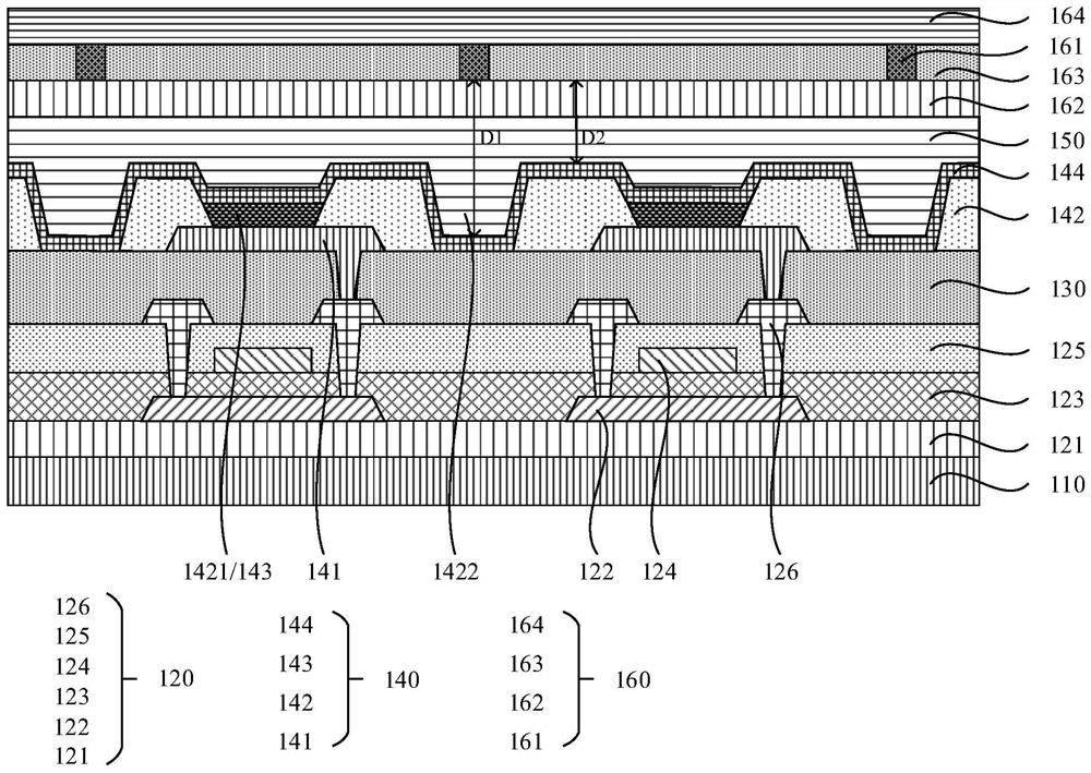
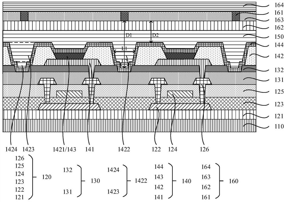
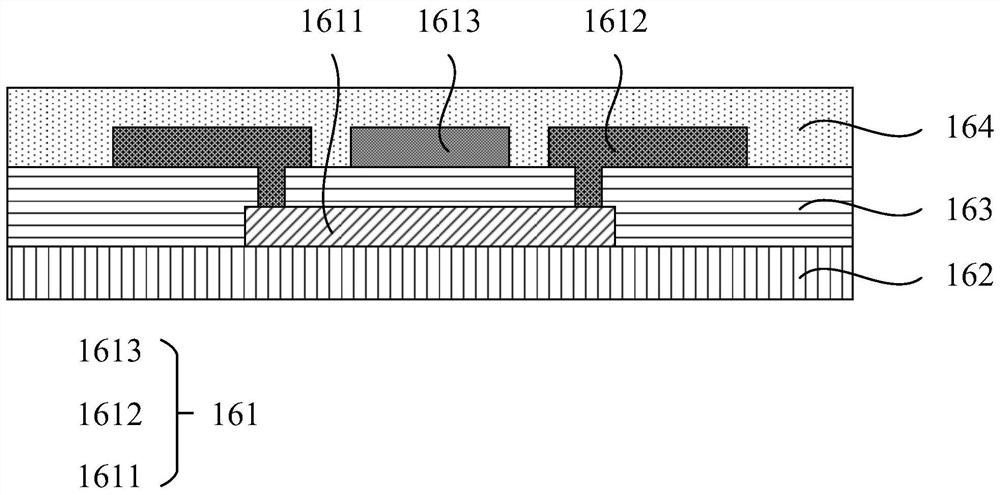
[0033] The technical solutions in the embodiments and / or examples of the application will be clearly and completely described below in conjunction with the specific embodiments of the application. Obviously, the embodiments and / or examples described below are only part of the implementation of the application. schemes and / or examples, rather than all implementations and / or examples. Based on the implementations and / or examples in this application, all other implementations and / or examples obtained by persons of ordinary skill in the art without making creative efforts belong to the protection scope of this application.

[0034] The directional terms mentioned in this application, such as [top], [bottom], [left], [right], [front], [back], [inside], [outside], [side], etc., are for reference only The orientation of the attached schema. Accordingly, the directional terms are used to illustrate and understand the application, not to limit the application. The terms "first", "sec...


PUM


Abstract

The invention provides an OLED display panel and a display device. The OLED display panel comprises a substrate; a driving circuit layer; a planarization layer; a light-emitting function layer which comprises a pixel electrode layer, a pixel definition layer, light-emitting material layers and a common electrode layer, and packaging layers and a touch layer, wherein the pixel definition layer is patterned to form pixel definition areas and grooves, the grooves are formed between at least two adjacent pixel definition areas, the light-emitting material layers are formed in the pixel definitionareas, and the common electrode layer is flatly laid on the pixel definition layer and the light-emitting material layers; the thickness of packaging layers in groove areas is greater than the thickness of packaging layers outside the groove areas and outside the pixel definition area; the touch layer comprises a touch electrode, the touch electrode is of a grid structure surrounding the pixel definition area, and the projection of the touch electrode on the substrate at least partially coincides with the projections of the grooves on the substrate. Therefore, the distance between the common electrode and the touch electrode is increased, the parasitic capacitance between the common electrode and the touch electrode is reduced, and the touch reporting rate and the touch sensitivity of theOLED display panel are improved.

Description

technical field [0001] The present application relates to the display field, in particular to an OLED display panel and a display device. Background technique [0002] Capacitive touch screens are widely used in various electronic interactive scene devices due to their high durability, long life, and support for multi-touch functions. The working principle of the capacitive touch screen is to detect the specific position touched by the finger by detecting the change of capacitance at the position touched by the finger. [0003] Currently for flexible AMOLED (Active-matrix organic light-emitting diode, active-matrix organic light-emitting diode or active-matrix organic light-emitting diode) On-cell (integrated touch layer on the AMOLED cover) display screen, its touch The control electrodes are usually made directly on the upper surface of the thin film encapsulation layer. However, due to the thin film encapsulation layer (usually thickness <10um), the distance between t...

Claims


Application Information

Patent Timeline
Patent Type & Authority Applications(China)
IPC IPC(8): H01L27/32G06F3/044
CPCG06F3/044H10K59/40H10K59/122G06F3/0446G06F3/0412H10K50/844H10K2102/351
Inventor 叶剑
Owner WUHAN CHINA STAR OPTOELECTRONICS SEMICON DISPLAY TECH CO LTD
Why Eureka
Try Eureka